US20020100029A1 - System, method and article of manufacture for compiling and invoking C functions in hardware - Google Patents
System, method and article of manufacture for compiling and invoking C functions in hardware Download PDFInfo
- Publication number
- US20020100029A1 US20020100029A1 US09/771,963 US77196301A US2002100029A1 US 20020100029 A1 US20020100029 A1 US 20020100029A1 US 77196301 A US77196301 A US 77196301A US 2002100029 A1 US2002100029 A1 US 2002100029A1
- Authority
- US
- United States
- Prior art keywords
- function
- fpga
- hardware
- software
- logic
- Prior art date
- Legal status (The legal status is an assumption and is not a legal conclusion. Google has not performed a legal analysis and makes no representation as to the accuracy of the status listed.)
- Abandoned
Links
Images


Classifications
-
- G—PHYSICS
- G06—COMPUTING; CALCULATING OR COUNTING
- G06F—ELECTRIC DIGITAL DATA PROCESSING
- G06F8/00—Arrangements for software engineering
- G06F8/40—Transformation of program code
- G06F8/41—Compilation
-
- G—PHYSICS
- G06—COMPUTING; CALCULATING OR COUNTING
- G06F—ELECTRIC DIGITAL DATA PROCESSING
- G06F8/00—Arrangements for software engineering
- G06F8/40—Transformation of program code
- G06F8/41—Compilation
- G06F8/44—Encoding
- G06F8/447—Target code generation
Definitions
- the present invention relates to a system for designing and producing an electronic circuit having a desired functionality and comprising both hardware which is dedicated to execution of certain of the functionality and software-controlled machines for executing the remainder of the functionality under the control of suitable software.
- a software-controlled processor is usually slower than hardware dedicated to that function.
- a way of overcoming this problem is to use a special software-controlled processor such as a RISC processor which can be made to function more quickly for limited purposes by having its parameters (for instance size, instruction set etc.) tailored to the desired functionality.
- a method and computer program product are provided for compiling a C function to a reconfigurable logic device.
- a function written in a C programming language is received.
- the C function is compiled into processor instructions, which are in turn used to generate hardware configuration information.
- the hardware configuration information is utilized to configure a Field Programmable Gate Array (FPGA) for compiling the function to the FPGA.
- FPGA Field Programmable Gate Array
- Handel-C is the preferred programming language for carrying out the methodology of the present invention and configuring the FPGA.
- a system for compiling a C function to a reconfigurable logic device includes receiving logic for receiving a function written in a C programming language. Compiling logic is used to compile the C function into processor instructions. Conversion logic generates hardware configuration information from the processor instructions. Configuring logic utilizes the hardware configuration information to configure an FPGA such that the function is compiled to the FPGA.
- the function is a shared function. More particularly, the function in the FPGA is shared amongst all its uses. In another embodiment of the present invention, the configuration of the FPGA is duplicated for each use, so that the function is used as an inline function. In yet another embodiment of the present invention, the FPGA is configured to provide an array of functions, where N copies of the function are specified for use M times.
- a token is used to invoke the function.
- the token is passed to a start signal, the start signal and call data are routed to the function, and the token is stored in a wait sub-circuit until the function is completed.
- FIG. 1 is a flow diagram of a process for automatically partitioning a behavioral description of an electronic system into the optimal configuration of hardware and software according to a preferred embodiment of the present invention
- FIG. 2 is a flow diagram schematically showing the codesign system of one embodiment of the invention.
- FIG. 3 illustrates the compiler objects which can be defined in one embodiment of the invention
- FIG. 4 is a block diagram of the platform used to implement the second example circuit produced by an embodiment of the invention.
- FIG. 5 is a picture of the circuit of FIG. 4;
- FIG. 6 is a block diagram of the system of FIG. 4;
- FIG. 7 is a simulation of the display produced by the example of FIGS. 4 to 6 ;
- FIG. 8 is a block diagram of a third example target system
- FIGS. 9 A-D are a block diagram showing a dependency graph for calculation of the variables in the FIG. 8 example.
- FIG. 10 is a schematic diagram of a hardware implementation of one embodiment of the present invention.
- FIG. 11 is a flow diagram of a process for compiling a C function to a reconfigurable logic device
- FIG. 12 is a diagram of a function call sub-circuit according to an embodiment of the present invention.
- FIG. 13 is an illustration of a pass by value sub-circuit according to one embodiment of the present invention.
- the present invention provides a hardware/software codesign system which can target a system in which the hardware or the processors to run the software can be customized according to the functions partitioned to it.
- the codesign system of this invention includes a partitioning means which flexibly decides the partitioning while varying the parameters of the hardware or processor to obtain both an optimal partitioning and optimal size of hardware and processor.
- the codesign system comprising means for receiving a specification of the functionality, partitioning means for partitioning implementation of the functionality between (a) and (b) and for customizing the hardware and/or the machine in accordance with the selected partitioning of the functionality.
- the target system is a hybrid hardware/software system. It can be formed using configurable logic resources in which case either the hardware or the processor, or both, can be formed on the configurable logic resources (e.g. an FPGA).
- configurable logic resources e.g. an FPGA
- the partitioning means uses a genetic algorithm to optimize the partitioning and the parameters of the hardware and the processor. Thus, it generates a plurality of different partitions of the functionality of the target system (varying the size of the hardware and/or the processor between the different partitions) and estimates the speed and size of the resulting system. It then selects the optimal partitioning on the basis of the estimates.
- a genetic algorithm a variety of partitions are randomly generated, the poor ones are rejected, and the remaining ones are modified by combining aspects of them with each other to produce different partitions. The speed and size of these are then assessed and the process can be repeated until an optimal partition is produced.
- the invention is applicable to target systems which use either customizable hardware and a customizable processor, or a fixed processor and customizable hardware, or fixed hardware and a customizable processor.
- the customizable part could be formed on an FPGA, or, for instance, an ASIC.
- the system may include estimators for estimating the speed and size of the hardware and the software controlled machine and may also include an interface generator for generating interfaces between the hardware and software. In that case the system may also include an estimator for estimating the size of the interface.
- the partitioning means calls the estimators when deciding on an optimum partitioning.
- the software-controlled machine can comprise a CPU and the codesign system comprises means for generating a compiler for the CPU as well as means for describing the CPU where it is to be formed on customizable logic circuits.
- the codesign system can further comprise a hardware compiler for producing from those parts of the specification partitioned to hardware a register transfer level description for configuring configurable logic resources (such as an FPGA). It can further include a synthesizer for converting the register transfer level description into a net list.
- a hardware compiler for producing from those parts of the specification partitioned to hardware a register transfer level description for configuring configurable logic resources (such as an FPGA). It can further include a synthesizer for converting the register transfer level description into a net list.
- the system can include a width adjuster for setting and using a desired data word size, and this can be done at several points in the desired process as necessary.
- Another aspect of the invention provides a hardware/software codesign system which receives a specification of a target system in the form of behavioral description, i.e. a description in a programming language such as can be written by a computer programmer, and partitions it and compiles it to produce hardware and software.
- behavioral description i.e. a description in a programming language such as can be written by a computer programmer
- the partitioning means can include a parser for parsing the input behavioral description.
- the description can be in a familiar computer language such as C, supplemented by a plurality of predefined attributes to describe, for instance, parallel execution of processes, an obligatory partition to software or an obligatory partition to hardware.
- the system is preferably adapted to receive a declaration of the properties of at least one of the hardware and the software-controlled machine, preferably in an object-oriented paradigm. It can also be adapted such that some parts of the description can be at the register transfer level, to allow closer control by the user of the final performance of the target system.
- the invention provides a hardware/software codesign system for making an electronic circuit which includes both dedicated hardware and software controlled resources.
- the codesign system receives a behavioral description of the target electronic system and automatically partitions the required functionality between hardware and software, while being able to vary the parameters (e.g. size or power) of the hardware and/or software.
- the hardware and the processor for the software can be formed on an FPGA, each being no bigger than is necessary to form the desired functions.
- the codesign system outputs a description of the required processor (which can be in the form of a net list for placement on the FPGA), machine code to run on the processor, and a net list or register transfer level description of the necessary hardware.
- the automatic partitioning can be performed by using an optimization algorithm, e.g. a genetic algorithm, which generates a partitioning based on estimates of performance.
- the invention also allows the manual partition of systems across a number of hardware and software resources from a single behavioral description of the system. This provision for manual partitioning, as well as automatic partitioning, gives the system great flexibility.
- the hardware resources may be a block that can implement random hardware, such as an FPGA or ASIC; a fixed processor, such as a microcontroller, DSP, processor, or processor core; or a customizable processor which is to be implemented on one of the hardware resources, such as an FPGA-based processor.
- the system description can be augmented with register transfer level descriptions, and parameterized instantiations of both hardware and software library components written in other languages.
- the sort of target systems which can be produced include:
- the use of the advanced estimation techniques in specific embodiments of the invention allows the system to take into account the area of the processor that will be produced, allowing the targeting of customizable processors with additional and removable instructions, for example.
- the estimators also take into account the speed degradation produced when the logic that a fixed hardware resource must implement nears the resource's size limit. This is done by the estimator reducing the estimated speed as that limit is reached. Further, the estimators can operate on both the design before partitioning, and after partitioning. Thus high level simulation, as well as simulation and estimation after partitioning, can be performed.
- the part of the system which compiles the software can transparently support additional or absent instructions for the processor and so is compatible with the parameterization of the processor.
- the input language supports variables with arbitrary widths, which are then unified to a fixed width using a promotion scheme, and then mapped to the widths available on the target system architecture.
- the input description may include both behavioral and register transfer level descriptions, which can both be compiled to software. This gives support for very fast simulation and allows the user control of the behavior of the hardware on each clock cycle.
- FIG. 1 is a flow diagram of a process 100 for automatically partitioning a behavioral description of an electronic system into the optimal configuration of hardware and software according to a preferred embodiment of the present invention.
- the system receives a behavioral description of the electronic system and, in operation 104 , determines the optimal required functionality between hardware and software.
- that functionality is partitioned preferably while varying the parameters (e.g. size or power) of the hardware and/or software.
- the hardware and the processors for the software can be formed on a reconfigurable logic device, each being no bigger than is necessary to form the desired functions.
- the codesign system outputs a description of the required processors, machine code to run on the processors, and a net list or register transfer level description of the necessary hardware. It is possible for the user to write some parts of the description of the system at register transfer level to give closer control over the operation of the system, and the user can specify the processor or processors to be used, and can change, for instance, the partitioner, compilers or speed estimators used in the codesign system.
- the automatic partitioning is formed by using a genetic algorithm which estimates the performance of randomly generated different partitions and selects an optimal one of them.
- Appendix 1 is an exemplary register transfer level description of a simple processor.
- Appendix 2 is a register transfer level description of the main process flow in the example of FIGS. 4 to 6 .
- Appendix 3 is the input specification for the target system of FIG. 8.
- the flow of the codesign process in an embodiment of the invention is shown in FIG. 2 and will be described below.
- the target architecture for this system is an FPGA containing one or more processors, and custom hardware.
- the processors may be of different architectures, and may communicate with each other and with the custom hardware.
- the user writes a description 202 of the system in a C-like language, which is actually ANSI C with some additions which allow efficient translation to hardware and parallel processes.
- This input description will be compiled by the system 200 of FIG. 2.
- the additions to the ANSI C language include the following:
- Variables are declared with explicit bit widths and the operators working on the variables work with an arbitrary precision. This allows efficient implementation in hardware. For instance a statement which declares the width of variables (in this case the program counter pc, the instruction register ir, and the top of stack tos) is as follows:
- the width of the data path of the processor in the target system may be declared, or else is calculated by the partitioner 208 as the width of the widest variable which it uses.
- the “par” statement has been added to describe process-level parallelism.
- the system can automatically extract fine-grained parallelism from the C-like description but generating coarse-grained parallelism automatically is far more difficult. Consequently the invention provides this attribute to allow the user to express parallelism in the input language using the “par” statement which specifies that a following list of statements is to be executed in parallel. For example, the expression: Par ⁇ parallel_port(port); SyncGeno; ⁇
- [0066] means that two sub-routines, the first of which is a driver for a parallel port and the second of which is a sync generator for a video display are to be executed in parallel. All parts of the system will react to this appropriately.
- Channels can be declared and are used for blocking, point-to-point synchronized communication as used in occam (see G. Jones. Programming in occam. Prentice Hall International Series in Computer Science, 1987, which is hereby incorporated by reference) with a syntax like a C function call.
- the parallel processes can use the channels to perform distributed assignment.
- parallel processes can communicate using blocking channel communication.
- the keyword “chan” I declares these channels. For example,
- [0071] is a statement which sends the value of variable a down channel 1; and receive (channel 2, b) is a statement which assigns the value received along channel 2 to variable b.
- the hardware resources available are declared.
- the resources may be a customizable processor, a fixed processor, or custom hardware.
- the custom hardware may be of a specific architecture, such as a Xilinx FPGA. Further, the architecture of the target system can be described in terms of the available functional units and their interconnection.
- a platform can be hard or soft.
- a hard platform is something that is fixed such as a Pentium processor or an FPGA.
- a soft platform is something that can be configured like an FPGA-based processor.
- the partitioner 208 understands the keywords “hard” and “soft”, which are used for declaring these platforms and the code can be implemented on any of these.
- Xilinx 4000 series FPGAs e.g. the Xilinx 4085 below
- An attribute can be attached to a platform when it is declared:
- the attribute PLATFORMS contains one element: the architecture of the hard platform. In this embodiment this may be the name of a Xilinx 3000 or 4000 series FPGA, an Altera FPGA, or an x86 processor.
- PLATFORMS is a pair.
- the first element is the architecture of the platform:
- Channels can be declared with an implementation, and as only being able to link previously declared platforms.
- the system 200 recognizes the following channel implementations:
- PCIBus a channel implemented over a PCI bus between an FPGA card and a PC host.
- FPGAChan a channel implemented using wires on the FPGA.
- CHANNELTYPE may be PCIBus or FPGAChan.
- FPGAChan is the default.
- PLATFORM is the name of the platform which can send down the channel.
- PLATFORM is the name of the platform which can receive from the channel.
- the system 200 checks that the declared channels and the platforms that use them are compatible.
- the communication mechanisms which a given type of channel can implement are built into the system. New mechanisms can be added by the user, in a similar way to adding new processors as will be explained below.
- Example Architecture [0099] Example Architecture /* Architectural Declarations */ // the 4085 is a hard platform -- call this one meetea board hard meeteaBoard -attribute_((platform(Xilinx4085))); // the pentium is a hard platform -- call this one hostProcessor hard hostProcessor attribute- ((platform(Pentium))); // proci is a soft platform which is implemented // on the FPGA on the meetea board soft proci attribute- ((platform(FpgaStackProc, meeteaBoard)));
- Attributes are also added to the input code to enable the user to specify whether a block is to be put in hardware or software and for software the attribute also specifies the target processor.
- the attribute also specifies whether the description is to be interpreted as a register transfer (RT) or behavioral level description.
- [0104] would be compiled to hardware using the RTL compiler, which would guarantee that the two assignments happened on the same clock cycle.
- PLATFORM is the name of the platform on which the code will be implemented. This implies the compiler which will be used to compile that code.
- LEVEL is Behavioral or RTL. Behavioral descriptions will be scheduled and may be partitioned. RTL descriptions are passed straight through to the RTL synthesizer e.g. a Handel-C compiler.
- NUMBER is a positive integer. Behavioral descriptions will be scheduled in such a way that the block of code will execute within that number of cycles, when possible. An error is generated if it is not possible.
- This input language is input to the parser 204 which parses and type checks the input code, and performs some syntax level optimizations, (in a standard way for parsers), and attaches a specific compiler to each block of code based on the attributes above.
- the parser 204 uses standard techniques [Aho, Sethi and Ullman; “Compilers Principles, Techniques, and Tools”; Addison Wesley known as “The Dragon Book”, which is hereby incorporated by reference] to turn the system description in the input language into an internal data structure, the abstract syntax tree which can be supplied to the partitioner 208 .
- the width adjuster 206 uses C-techniques to promote automatically the arguments of operators to wider widths such that they are all of the same width for instance by concatenating them with zeros. Thus this is an extension of the promotion scheme of the C language, but uses arbitrary numbers of bits. Further adjustment is carried out later in the flow at 206 a and 206 b, for instance by ANDing them with a bit mask. Each resource has a list of widths that it can support. For example a 32 bit processor may be able to carry out 8, 16 and 32 bit operations. Hardware may be able to support any width, or a fixed width datapath operator may have been instantiated from a library.
- the later width adjustment modules 206 a and 206 b insert commands to enable the width of operation in the description to be implemented correctly using the resources available.
- the partitioner 208 generates a control/data-flow graph (CDFG) from the abstract syntax tree, for instance using the techniques described in G. de Michelli “Synthesis and Optimization of Digital Circuits”; McGraw-Hill, 1994 which is hereby incorporated by reference. It then operates on the parts of the description which have not already been assigned to resources by the user. It groups parts of the description together into blocks, “partitioning blocks”, which are indivisible by the partitioner. The size of these blocks is set by the user, and can be any size between a single operator, and a top-level process. Small blocks tend to lead to a slow more optimal partition; large blocks tend to lead to a faster less optimal partition.
- CDFG control/data-flow graph
- the algorithm implemented in this embodiment of the system is a genetic algorithm for instance as explained in D. E. Goldberg, “Genetic Algorithms in Search, Optimization and Machine learning”, Addison-Wesley, 1989 which is hereby incorporated by reference.
- the resource on which each partitioning block is to be placed represents a gene and the fitness function returns infinity for a partitioning which the estimators say will not fit in the available hardware; otherwise it returns the estimated system speed. Different partitions are generated and estimated speed found.
- the user may set the termination condition to one of the following:
- the partitioner 208 uses estimators 220 , 222 , and 224 to estimate the size and speed of the hardware, software and interfaces as described below.
- the estimators and the simulation and profiling module 220 can accept a system description from any level in the flow.
- the input description which may include behavioral and register transfer level parts, to be compiled to software for simulation and estimation at this stage.
- the simulator can be used to collect profiling information for sets of typical input data, which will be used by the partitioner 208 to estimate data dependent values, by inserting data gathering operations into the output code.
- the estimator 222 is called by the partitioner 208 for a quick estimation of the size and speed of the hardware parts of the system using each partition being considered. Data dependent values are estimated using the average of the values for the sets of typical input data supplied by the user.
- the description is scheduled using a call to the behavioral synthesizer 212 .
- the user can choose which estimation algorithm to use, which gives a choice between slow accurate estimation and faster less accurate estimation.
- the speed and area of the resulting RTL level description is then estimated using standard techniques. For FPGAs the estimate of the speed is then decreased by a non-linear factor determined from the available free area, to take into account the slower speed of FPGA designs when the FPGA is nearly full.
- the target is customizable processors to be compiled by the system itself then a more accurate estimation of the software speed is used which models the optimizations that the software compiler 216 uses.
- the area and cycle time of the processor is modeled using a function which is written for each processor, and expresses the required values in terms of the values of the processor's parameterizations, such as the set of instructions that will be used, the data path and instruction register width and the cache size.
- Interfaces between the hardware and software are instantiated by the interface cosynthesizer 210 from a standard library of available communication mechanisms. Each communication mechanism is associated with an estimation function, which is used by the partitioner to cost the software and hardware speed and area required for given communication, or set of communications. Interfaces which are to be implemented using a resource which can be parameterized (such as a channel on an FPGA), are synthesized using the parameterizations decided by the partitioner. For example, if a transfer of ten thousand 32 bit values over a PCI bus was required, a DMA transfer from the host to an FPGA card's local memory might be used.
- the compiler parts of the system are designed in an object oriented way, and actually provide a class hierarchy of compilers, as shown in FIG. 3. Each node in the tree shows a class which is a subclass of its parent node.
- the top-level compiler class 302 provides methods common to both the hardware and software flows, such as the type checking, and a system-level simulator used for compiling and simulating the high-level description. These methods are inherited by the hardware and software compilers 304 , 306 , and may be used or overridden.
- the compiler class also specifies other, virtual, functions which must be supplied by its subclasses. So the compile method on the hardware compiler class compiles the description to hardware by converting the input description to an RTL description; the compile method on the Processor A compiler compiles a description to machine code which can run on Processor A.
- the compiler is called from the command line by the attributes mentioned above specifying which compiler to use for a block of code.
- A) Interactively An interactive environment is provided, where the user has access to a set of functions which the user can call, e.g. to estimate speed and size of hardware and software implementations, manually attach a compiler to a block of code, and call the simulator.
- This interactive environment also allows complex scripts, functions and macros to be written and saved by the user for instance so that the user can add a new partitioning algorithm.
- the main compilation stages of the process flow are software or hardware specific. Basically at module 212 the system schedules and allocates any behavioral parts of the hardware description, and at module 216 compiles the software description to assembly code. At module 218 it also writes a parameterized description of the processors to be used, which may also have been designed by the user. These individual steps will be explained in more detail.
- the parts of the description to be compiled into hardware use a behavioral synthesis compiler 212 using the techniques of De Michelli mentioned above.
- the description is translated to a control/data flow graph, scheduled (i.e. what happens on each clock cycle is established) and bound (i.e. which resources are used for which operations is established), optimized, and then an RT-level description is produced.
- the result of the hardware compilation by the behavioral synthesizer 212 is an RTL description which can be output to a RTL synthesis system 214 using a hardware description language (e.g. Handel-C or VHDL), or else synthesized to a gate level description using the techniques of De Michelli.
- a hardware description language e.g. Handel-C or VHDL
- RTL synthesis optimizes the hardware description, and maps it to a given technology. This is performed using standard techniques.
- the software compiler 216 largely uses standard techniques [e.g. from Aho, Sethi and Ullman mentioned above].
- parallelism is supported by mapping the invention's CSP-like model of parallelism and communication primitives into the target model. For instance channels can mapped to blocks of shared memory protected by semaphores.
- CSP is described in C. A. R. Hoare “Communicating sequential processes.” Prentice-Hall International series in computing science. Prentice-Hall International, Englewood Cliffs, N.J. which is hereby incorporated by reference.
- the software compiler is organized in an object oriented way to allow users to add support for different processors (see FIG. 3) and for processor parameterizations. For example, in the processor parameterize 218 unused instructions from the processor description are automatically removed, and support for additional instructions can be added.
- This embodiment of the invention includes some prewritten processor descriptions which can be selected by the user. It contains parameterized descriptions of three processors, and the software architecture is designed so that it is easy for developers to add new descriptions which can be completely new or refinements of these.
- the three processors provided are
- a 2-cycle non-pipelined stack-based processor (see below).
- a more sophisticated multicycle non-pipelined stack-based processor with a variable number of cycles per instruction, and hardware support for parallelism and channels.
- the software compiler supports many processor parameterizations. More complex and unexpected modifications are supported by virtue of the object oriented design of the compiler, which allows small additions to be made easily by the user. Most of the mapping functions can be inherited from existing processor objects, minor additions can be made a function used to calculate the speed and area of processor given the parameterizations of the processor and a given program.
- the output of the software compilation/processor parameterization process is machine code to run on the processor together with a description of the processor to be used (if it is not a standard one).
- Handel-C provides estimation of the speed and area of the design, which is written as an HTML file to be viewed using a standard browser, such as Netscape.
- the file shows two versions of the program: in one each statement is colored according to how much area it occupies, and in the other according to how much combinational delay it generates. The brighter the color for each statement, the greater the area or delay. This provides a quick visual feedback to the user of the consequences of design decisions.
- the Handel-C simulator is a fast cycle-accurate simulator which uses the C-like nature of the specification to produce an executable which simulates the design. It has an X-windows interface which allows the user to view VGA video output at about one frame per second.
- the simulator can be used to collect profiling information for sets of typical input data, which will be used by the partitioner 208 to estimate data dependent values, by inserting data gathering operations into the output code.
- a subset of the above system could be used to provide a provably correct compilation strategy. This subset would include the channel communication and parallelism of OCCAM and CSP. A formal semantics of the language could be used together with a set of transformations and a mathematician, to develop a provably correct partitioning and compilation route.
- the description of the processor to be used to run the software part of the target system may itself be written in the C-like input language and compiled using the codesign system. As it is such an important element of the final design most users will want to write it at the register transfer level, in order to hand-craft important parts of the design. Alternatively the user may use the predefined processors, provided by the codesign system or write the description in VHDL or even at gate level, and merge it into the design using an FPGA vendor's tools.
- the first processor parameterization to consider is removing redundant logic. Unused instructions can be removed, along with unused resources, such as the floating point unit or expression stack.
- the second parameterization is to add resources. Extra RAMS and ROMs can be added.
- the instruction set can be extended from user assigned instruction definitions. Power-on bootstrap facilities can be added.
- the third parameterization is to tune the size of the used resources.
- the bit widths of the program counter, stack pointer, general registers and the opcode and operand portions of the instruction register can be set.
- the size of internal memory and of the stack or stacks can be set, the number and priorities of interrupts can be defined, and channels needed to communicate with external resources can be added. This freedom to add communication channels is a great benefit of codesign using a parametrizable processor, as the bandwidth between hardware and software can be changed to suit the application and hardware/software partitioning.
- the processor starts with a definition of the instruction width, and the width of the internal memory and stack addresses. This is followed by an assignment of the processor opcodes. Next the registers are defined; the declaration “unsigned x y, z” declares unsigned integers y and z of width x.
- the program counter, instruction register and top-of-stack are the instruction width; the stack pointer is the width of the stack.
- the processor is defined. This is a simple non-pipelined two-cycle processor. On the first cycle (the first three-line “par”), the next instruction is fetched from memory, the program counter is incremented, and the top of the stack is saved. On the second cycle the instruction is decoded and executed. In this simple example a big switch statement selects the fragment of code which is to be executed.
- This simple example illustrates a number of points.
- Various parameters such as the width of registers and the depth of the stack can be set. Instructions can be added by including extra cases in the switch statement. Unused instructions and resources can be deleted, and opcodes can be assigned.
- the example also introduces a few other features of the register transfer level 30 language such as rom and ram declarations.
- the target system is a video game in which the user can fly a plane over a detailed background picture. Another user can be dialed up, and the screen shows both the local plane and a plane controlled remotely by the other user.
- the main challenge for the design is that the system must be implemented on a single medium-sized FPGA.
- the platform for this application was a generic and simple FPGA-based board.
- a block diagram of the board 400 is shown in FIG. 4, and a graphical depiction of the board 400 is shown in FIG. 5.
- the Hammond board contains a Xilinx 4000 series FPGA and 256 kb synchronous static RAM. Three buttons provide a simple input device to control the plane; alternatively a standard computer keyboard can be plugged into the board. There is a parallel port which is used to configure the FPGA, and a serial port. The board can be clocked at 20 MHz from a crystal, or from a PLL controlled by the FPGA. Three groups of four pins of the FPGA are connected to a resistor network which gives a simple digital to analogue converter, which can be used to provide 12 bit VGA video by implementing a suitable sync generator on the FPGA. Problem description and discussion The specification of the video game system is as follows:
- the system must dial up an Internet service provider, and establish a connection with the remote game. which will be running on a workstation.
- the system must display a reconfigurable background picture.
- the system must display on a VGA monitor a picture of two planes: the local plane and the remote plane.
- the position of the local plane will be controlled by the buttons on the Hammond board.
- This simple problem combines some hard timing constraints, such as sending a stream of video to the monitor, with some complex tasks without timing constraints, such as connecting to the Internet service provider. There is also an illustration of contention for a shared resource, which will be discussed later.
- a block diagram of the system 600 is shown in FIG. 6.
- the system design decisions were quite straightforward.
- a VGA monitor 602 is plugged straight into the Hammond board 400 .
- a modem 604 can be used, and plugged into the serial port of the Hammond board. Otherwise it is quite feasible to build a simple modem in the FPGA.
- a simple way of generating the video is to build a sync generator in the FPGA, and calculate and output each pixel of VGA video at the pixel rate.
- the background picture can be stored in a “picture RAM”.
- the planes can be stored.
- the hardware portions of the design are dictated by the need of some part of the system to meet tight timing constraints. These are the video generation circuitry and the port drivers. Consequently these were allocated to hardware, and their C descriptions written at register transfer level to enable them to meet the timing constraints.
- the picture RAM and the character generator ROM and character location RAM were all stored in the Hammond board RAM bank as the size estimators showed that there would be insufficient space on the FPGA.
- the parts of the design to be implemented in software are the dial-up and negotiation, establishing the network, and communicating the plane locations. These are non-time critical, and so can be mapped to software.
- the program is stored in the RAM bank, as there is not space for the application code in the FPGA.
- the main function is shown in Appendix 2. The first two lines declare some communication channels. Then the driver for the parallel port and sync generator are started, and the RAM is initialized with the background picture, the character memory and the program memory. The parallel communicating hardware and software process are then started, communicating over a channel hwswchan. The software establishes the network connection, and then enters a loop which transmits and receives the position of the local and remote plane, and sends new positions to the display process.
- the simple stack-based processor from Appendix 1 was parameterized in the following ways to run this software.
- the width of the processor was made to be 10 bits, which is sufficient to address a character on the screen in a single word. No interrupts were required, so these were removed, as were a number of unused instructions, and the internal memory.
- the RT-level design was simulated using the Handel-C simulator. Sample input files mimicking the expected inputs from the peripherals were prepared, and these were fed into the simulator. A black and white picture 700 of the color display is shown in FIG. 7 (representing a snapshot of the X window drawn by the co-simulator).
- This application would not have been easy to implement without the codesign system of the invention.
- a hardware-only solution would not have fitted. onto the FPGA; a software-only solution would not have been able to generate the video and interface with the ports at the required speed.
- the invention allows the functionality of the target system to be partitioned while parameterizing the processor to provide an optimal system.
- the display process needs to be able to access the memory without delay, because of the tight timing constraints placed on it.
- a semaphore is used to indicate when the display process requires the memory. In this case the processor stalls until the semaphore is lowered. On the next cycle the processor then presents to the memory the address of the next instruction, which in some cases may already have been presented once.
- the “springs” program is a small example of a codesign programmed in the C-like language mentioned above. It performs a simulation of a simple mass-spring system, with a real time display on a monitor, and interaction via a pair of buttons.
- the design consists of three parts: a process computing the motion of the masses, a process rendering the positions of the masses into line segments, and a process which displays these segments and supplies the monitor with appropriate synchronization signals.
- the first two processes are written in a single C-like program.
- the display process is hard real-time and so requires a language which can control external signals at the resolution of a single clock cycle, so for this reason it is implemented using an RTL description (Handel-C in this instance).
- FIG. 8 is a block diagram of the ultimate implementation, together with a representation of the display of the masses and springs.
- FIG. 9 is a dependency graph for calculation of the variables required.
- the mass motion process first sets up the initial positions, velocities and acceleration of the masses. This can be seen in Appendix 3 where positions p 0 to p 7 are initialized as 65536.
- the program then continues in an infinite loop, consisting of: sending pairs of mass positions to the rendering process, computing updated positions based on the velocities of the masses, computing updated velocities based on the accelerations of the masses, and computing accelerations based on the positions of the masses according to Hooke's law.
- the process then reads the status of the control buttons and sets the position of one of the masses accordingly. This can be seen in Appendix 3 as the statement “received (buttons, button status)”.
- the rendering process runs an infinite loop performing the following operations: reading a pair of mass positions from the mass motion process then interpolate in between these two positions for the next 64 lines of video output. A pair of interpolated positions is sent to the RTL display process once per line. This is a relatively simple process with only one calculation, but this must be performed very regularly.
- the display process (which is written in Handel-C) and is illustrated in Appendix 3 reads start and end positions from the rendering process and drives the video color signal between these positions on a scan line. Simultaneously, it drives the synchronization signals for the monitor. At the end of each frame it reads the values from the external buttons and sends these to the mass motion process.
- the design could be partitioned it in a large number of ways. It could partition the entire design into hardware or into software, partition the design at the high-level, by the first two processes described above and compiling them using one of the possible routes, or it can partition the design at a lower level, and generate further parallel processes communicating with each other. Whatever choice the partitioner makes, it maintains the functional correctness of the design, but will change the cost of the implementation (in terms of the area, clock cycles and so forth). The user may direct the partitioner to choose one of the options above the others. A number of the options are described below.
- the partitioner could map the first two processes directly into Handel-C, after performing some additional parallelization.
- the problem with this approach is that each one of the operations in the mass motion process will be dedicated to its own piece of hardware, in an effort to increase performance. However, as discussed above, this is unnecessary as these calculations can be performed at a slower speed.
- the result is a design that can perform quickly enough but which is too large to fit on a single FPGA. This problem would be recognized by the partitioner using its area estimation techniques.
- partitioner Another alternative would be for the partitioner to generate a pair of parameterized processors running in parallel, the first calculating motion and the second performing the rendering.
- the area required is still smaller than the pure hardware approach, and the speed is now sufficient to implement the system in real time.
- using a parameterized processor for the rendering process adds some overhead (for instance, performing the instruction decoding), which is unnecessary. So although the solution works, it is a sub optimal.
- the best solution, and the one chosen by the partitioner, is to partition the mass motion process into software for a parameterized, unthreaded processor, and to partition the rendering process 810 which was written at a behavioral level together with the position, velocity and acceleration calculations 806 into hardware.
- This solution has the minimum area of the options considered, and performs sufficiently quickly to satisfy the real time display process.
- the behavioral part of the system 802 includes the calculation of the positions, velocities and accelerations of the masses at 806 (which will subsequently be partitioned to software), and the line and drawing processes at 810 (which will subsequently be partitioned to hardware).
- the RTL hardware 820 is used to receive the input from the buttons at 822 and output the video at 824 .
- the partitioner 208 used the estimators 220 , 222 and 224 to estimate the speed and area of each possible partition based on the use of a customized processor.
- the interface cosynthesizer 210 implements the interface between hardware and software on two FPGA channels 804 and 808 and these are used to transfer a position information to the rendering process and to transfer the button information to the position calculation 806 from button input 822 .
- the width adjuster 206 which is working on the mass motion part of the problem to be partitioned to software, parameterizes the processor to have a width of 17 bits and adjusts the width of “curr_pos” which is the current position to nine bits, the width of the segment channel.
- the processor parameterize at 17 further parameterizes the processor by removing unused instructions such as multiply, interrupts, and the data memory is reduced and multi-threading is removed. Further, op codes are assigned and the operator width is adjusted.
- the partitioner 208 generates a dependency graph as shown in FIG. 9 which indicates which variables depend on which. It is used by the partitioner to determine the communications costs associated with the partitioning, for instance to assess the need for variables to be passed from one resource to another given a particular partitioning.
- FIG. 10 illustrates a typical hardware configuration of a workstation in accordance with a preferred embodiment having a central processing unit 1010 , such as a microprocessor, and a number of other units interconnected via a system bus 1012 .
- a central processing unit 1010 such as a microprocessor
- FIG. 10 illustrates a typical hardware configuration of a workstation in accordance with a preferred embodiment having a central processing unit 1010 , such as a microprocessor, and a number of other units interconnected via a system bus 1012 .
- RAM 1014 Random Access Memory (RAM) 1014 , Read Only Memory (ROM) 1016 , an I/O adapter 1018 for connecting peripheral devices such as disk storage units 1020 to the bus 1012 , a user interface adapter 1022 for connecting a keyboard 1024 , a mouse 1026 , a speaker 1028 , a microphone 1032 , and/or other user interface devices such as a touch screen (not shown) to the bus 1012 , communication adapter 1034 for connecting the workstation to a communication network (e.g., a data processing network) and a display adapter 1036 for connecting the bus 1012 to a display device 1038 .
- a communication network e.g., a data processing network
- display adapter 1036 for connecting the bus 1012 to a display device 1038 .
- the workstation typically has resident thereon an operating system such as the Microsoft Windows NT or Windows/95 Operating System (OS), the IBM OS/2 operating system, the MAC OS, or UNIX operating system.
- OS Microsoft Windows NT or Windows/95 Operating System
- IBM OS/2 operating system the IBM OS/2 operating system
- MAC OS the MAC OS
- UNIX operating system the operating system
- a preferred embodiment is written using JAVA, C, and the C++ language and utilizes object oriented programming methodology.
- Object oriented programming has become increasingly used to develop complex applications.
- OOP Object oriented programming
- OOP is a process of developing computer software using objects, including the steps of analyzing the problem, designing the system, and constructing the program.
- An object is a software package that contains both data and a collection of related structures and procedures. Since it contains both data and a collection of structures and procedures, it can be visualized as a self-sufficient component that does not require other additional structures, procedures or data to perform its specific task.
- OOP therefore, views a computer program as a collection of largely autonomous components, called objects, each of which is responsible for a specific task. This concept of packaging data, structures, and procedures together in one component or module is called encapsulation.
- OOP components are reusable software modules which present an interface that conforms to an object model and which are accessed at run-time through a component integration architecture.
- a component integration architecture is a set of architecture mechanisms which allow software modules in different process spaces to utilize each others capabilities or functions. This is generally done by assuming a common component object model on which to build the architecture. It is worthwhile to differentiate between an object and a class of objects at this point.
- An object is a single instance of the class of objects, which is often just called a class.
- a class of objects can be viewed as a blueprint, from which many objects can be formed.
- OOP allows the programmer to create an object that is a part of another object.
- the object representing a piston engine is said to have a composition-relationship with the object representing a piston.
- a piston engine comprises a piston, valves and many other components; the fact that a piston is an element of a piston engine can be logically and semantically represented in OOP by two objects.
- OOP also allows creation of an object that “depends from” another object. If there are two objects, one representing a piston engine and the other representing a piston engine wherein the piston is made of ceramic, then the relationship between the two objects is not that of composition.
- a ceramic piston engine does not make up a piston engine. Rather it is merely one kind of piston engine that has one more limitation than the piston engine; its piston is made of ceramic.
- the object representing the ceramic piston engine is called a derived object, and it inherits all of the aspects of the object representing the piston engine and adds further limitation or detail to it.
- the object representing the ceramic piston engine “depends from” the object representing the piston engine. The relationship between these objects is called inheritance.
- the object or class representing the ceramic piston engine inherits all of the aspects of the objects representing the piston engine, it inherits the thermal characteristics of a standard piston defined in the piston engine class.
- the ceramic piston engine object overrides these ceramic specific thermal characteristics, which are typically different from those associated with a metal piston. It skips over the original and uses new functions related to ceramic pistons.
- Different kinds of piston engines have different characteristics, but may have the same underlying functions associated with it (e.g., how many pistons in the engine, ignition sequences, lubrication, etc.).
- a programmer would call the same functions with the same names, but each type of piston engine may have different/overriding implementations of functions behind the same name. This ability to hide different implementations of a function behind the same name is called polymorphism and it greatly simplifies communication among objects.
- Objects can represent physical objects, such as automobiles in a traffic-flow simulation, electrical components in a circuit-design program, countries in an economics model, or aircraft in an air-traffic-control system.
- Objects can represent elements of the computer-user environment such as windows, menus or graphics objects.
- An object can represent an inventory, such as a personnel file or a table of the latitudes and longitudes of cities.
- An object can represent user-defined data types such as time, angles, and complex numbers, or points on the plane.
- OOP allows the software developer to design and implement a computer program that is a model of some aspects of reality, whether that reality is a physical entity, a process, a system, or a composition of matter. Since the object can represent anything, the software developer can create an object which can be used as a component in a larger software project in the future.
- C++ is an OOP language that offers a fast, machine-executable code.
- C++ is suitable for both commercial-application and systems-programming projects.
- C++ appears to be the most popular choice among many OOP programmers, but there is a host of other OOP languages, such as Smalltalk, Common Lisp Object System (CLOS), and Eiffel. Additionally, OOP capabilities are being added to more traditional popular computer programming languages such as Pascal.
- Encapsulation enforces data abstraction through the organization of data into small, independent objects that can communicate with each other. Encapsulation protects the data in an object from accidental damage, but allows other objects to interact with that data by calling the object's member functions and structures.
- Class hierarchies and containment hierarchies provide a flexible mechanism for modeling real-world objects and the relationships among them.
- Class libraries are very flexible. As programs grow more complex, more programmers are forced to adopt basic solutions to basic problems over and over again. A relatively new extension of the class library concept is to have a framework of class libraries. This framework is more complex and consists of significant collections of collaborating classes that capture both the small scale patterns and major mechanisms that implement the common requirements and design in a specific application domain. They were first developed to free application programmers from the chores involved in displaying menus, windows, dialog boxes, and other standard user interface elements for personal computers.
- Frameworks also represent a change in the way programmers think about the interaction between the code they write and code written by others.
- the programmer called libraries provided by the operating system to perform certain tasks, but basically the program executed down the page from start to finish, and the programmer was solely responsible for the flow of control. This was appropriate for printing out paychecks, calculating a mathematical table, or solving other problems with a program that executed in just one way.
- event loop programs require programmers to write a lot of code that should not need to be written separately for every application.
- the concept of an application framework carries the event loop concept further. Instead of dealing with all the nuts and bolts of constructing basic menus, windows, and dialog boxes and then making these things all work together, programmers using application frameworks start with working application code and basic user interface elements in place. Subsequently, they build from there by replacing some of the generic capabilities of the framework with the specific capabilities of the intended application.
- Application frameworks reduce the total amount of code that a programmer has to write from scratch.
- the framework is really a generic application that displays windows, supports copy and paste, and so on, the programmer can also relinquish control to a greater degree than event loop programs permit.
- the framework code takes care of almost all event handling and flow of control, and the programmer's code is called only when the framework needs it (e.g., to create or manipulate a proprietary data structure).
- a programmer writing a framework program not only relinquishes control to the user (as is also true for event loop programs), but also relinquishes the detailed flow of control within the program to the framework. This approach allows the creation of more complex systems that work together in interesting ways, as opposed to isolated programs, having custom code, being created over and over again for similar problems.
- a framework basically is a collection of cooperating classes that make up a reusable design solution for a given problem domain. It typically includes objects that provide default behavior (e.g., for menus and windows), and programmers use it by inheriting some of that default behavior and overriding other behavior so that the framework calls application code at the appropriate times.
- default behavior e.g., for menus and windows
- Behavior versus protocol Class libraries are essentially collections of behaviors that you can call when you want those individual behaviors in your program.
- a framework provides not only behavior but also the protocol or set of rules that govern the ways in which behaviors can be combined, including rules for what a programmer is supposed to provide versus what the framework provides.
- a preferred embodiment of the invention utilizes HyperText Markup Language (HTML) to implement documents on the Internet together with a general-purpose secure communication protocol for a transport medium between the client and the Newco. HTTP or other protocols could be readily substituted for HTML without undue experimentation.
- HTML HyperText Markup Language
- RRC 1866 Hypertext Markup Language—2.0
- HTML Hypertext Transfer Protocol—HTTP/1.1: HTTP Working Group Internet Draft
- HTML documents are SGML documents with generic semantics that are appropriate for representing information from a wide range of domains. HTML has been in use by the World-Wide Web global information initiative since 1990. HTML is an application of ISO Standard 8879; 1986 information Processing Text and Office Systems; Standard Generalized Markup Language (SGML).
- HTML has been the dominant technology used in development of Web-based solutions.
- HTML has proven to be inadequate in the following areas:
- UI User Interface
- Custom “widgets” e.g., real-time stock tickers, animated icons, etc.
- client-side performance is improved.
- Java supports the notion of client-side validation, offloading appropriate processing onto the client for improved performance.
- Dynamic, real-time Web pages can be created. Using the above-mentioned custom Ul components, dynamic Web pages can also be created.
- Sun's Java language has emerged as an industry-recognized language for “programming the Internet.”
- Sun defines Java as: “a simple, object-oriented, distributed, interpreted, robust, secure, architecture-neutral, portable, high-performance, multithreaded, dynamic, buzzword-compliant, general-purpose programming language.
- Java supports programming for the Internet in the form of platform-independent Java applets.”
- Java applets are small, specialized applications that comply with Sun's Java Application Programming Interface (API) allowing developers to add “interactive content” to Web documents (e.g., simple animations, page adornments, basic games, etc.).
- Applets execute within a Java-compatible browser (e.g., Netscape Navigator) by copying code from the server to client. From a language standpoint, Java's core feature set is based on C++. Sun's Java literature states that Java is basically, “C++ with extensions from Objective C for more dynamic method resolution.”
- ActiveX includes tools for developing animation, 3-D virtual reality, video and other multimedia content.
- the tools use Internet standards, work on multiple platforms, and are being supported by over 100 companies.
- the group's building blocks are called ActiveX Controls, small, fast components that enable developers to embed parts of software in hypertext markup language (HTML) pages.
- ActiveX Controls work with a variety of programming languages including Microsoft Visual C++, Borland Delphi, Microsoft Visual Basic programming system and, in the future, Microsoft's development tool for Java, code named “Jakarta.”
- ActiveX Technologies also includes ActiveX Server Framework, allowing developers to create server applications.
- ActiveX could be substituted for JAVA without undue experimentation to practice the invention.
- the codesign system of the invention has the following advantages in designing a target system:
- the hardware can be designed to run in parallel with the processors to meet speed constraints. Thus time critical parts of the system can be allocated to custom hardware, which can be designed at the behavioral or register transfer level.
- Non-time critical parts of the design can be allocated to software, and run on a small, slow processor.
- the system can target circuitry on dynamic FPGAs.
- the FPGA can contain a small processor which can configure and reconfigure the rest of the FPGA at run time.
- FIG. 11 depicts a process 1100 for compiling a C function to a reconfigurable logic device.
- a function written in a C programming language is received.
- the C function is compiled into processor instructions in operation 1104 .
- the processor instructions are used to generate hardware configuration information.
- a Field Programmable Gate Array (FPGA) is configured using the hardware configuration information such that the function is compiled to the FPGA. Note that the methodology of the present invention could also be applied to compile functions to reconfigurable logic devices other than FPGAs.
- a system for compiling a C function to a reconfigurable logic device includes receiving logic for receiving a function written in a C programming language. Compiling logic is used to compile the C function into processor instructions. Conversion logic generates hardware configuration information from the processor instructions. Configuring logic utilizes the hardware configuration information to configure an FPGA such that the function is compiled to the FPGA.
- the function is a shared function. More particularly, the function in the FPGA is shared amongst all its uses. In another embodiment of the present invention, the configuration of the FPGA is duplicated for each use, so that the function is used as an inline function. In yet another embodiment of the present invention, the FPGA is configured to provide an array of functions, where N copies of the function are specified for use M times.
- a token is used to invoke the function.
- the token is passed to a start signal, the start signal and call data are routed to the function, and the token is stored in a wait sub-circuit until the function is completed.
- Handel-C is the preferred programming language for carrying out the methodology of the present invention and configuring the FPGA.
- One skilled in the art will be familiar with programming in Handel-C and therefore only a general discussion of Handel-C will be provided. Handel-C is described in more detail below in the section entitled “Handel-C.”
- FIG. 12 illustrates the control logic 1200 for calling (invoking) functions which are shared.
- Handel-C circuits are generally controlled by tokens.
- a function is called by passing a token to the START signal 1202 .
- the multiplexer 1204 routes the START signal and associated data from this call to the implementation of the function body 1206 .
- the token is stored in a “wait sub-circuit” 1208 .
- the wait sub-circuit includes an OR gate 1212 , an AND gate 1214 with an inverter, a second AND gate 1216 , and a flip-flop 1218 which stores the token.
- the DONE signal 1210 is asserted and the token is passed to the circuitry following this invocation of the function.
- FIG. 13 depicts a pass by value sub-circuit 1300 according to an embodiment of the present invention. Passing by value uses the circuit which, on the first clock cycle of the function body 1206 (see FIG. 12), copies the values of the arguments into temporary variables, unless those parameters are written to in the first clock cycle, in which case the value being written is stored in the variable in that cycle.
- the temporary variable is stored in a storage medium 1302 , which can include memory or reconfigurable logic for example.
- Gating logic 1304 handles the write to the temporary variable. Note that the gating logic includes several AND and OR gates.
- a multiplexer 1306 handles the read from the parameter, wich is either a temporary variable or the value passed in. FIRST is a signal that is true if it is the first clock cycle of the function call.
- D A is the argument to the function.
- D 1 and D 2 are the other data written to the variable, together with the associated write enables (WE).
- FPLD Field-Programmable Logic Devices
- PAL Programmable Array Logic device
- CPLD Complex PLD's
- This paradigm is characterized by devices such as the Advanced Micro Devices MACH.TM. family.
- Examples of CPLD circuitry are seen in U.S. Pat. No. 5,015,884 (issued May 14, 1991 to Om P. Agrawal et al.) and U.S. Pat. No. 5,151,623 (issued Sep. 29, 1992 to Om P. Agrawal et al.), which are herein incorporated by reference.
- FPGA Field Programmable Gate Arrays
- Examples of such devices include the XC2000.TM. and XC3000.TM. families of FPGA devices introduced by Xilinx, Inc. of San Jose, Calif.
- the architectures of these devices are exemplified in U.S. Pat. Nos. 4,642,487; 4,706,216; 4,713,557; and 4,758,985; each of which is originally assigned to Xilinx, Inc. and which are herein incorporated by reference for all purposes.
- An FPGA device can be characterized as an integrated circuit that has four major features as follows.
- a user-accessible, configuration-defining memory means such as SRAM, PROM, EPROM, EEPROM, anti-fused, fused, or other, is provided in the FPGA device so as to be at least once-programmable by device users for defining user-provided configuration instructions.
- Static Random Access Memory or SRAM is of course, a form of reprogrammable memory that can be differently programmed many times.
- Electrically Erasable and reProgrammable ROM or EEPROM is an example of nonvolatile reprogrammable memory.
- the configuration-defining memory of an FPGA device can be formed of mixture of different kinds of memory elements if desired (e.g., SRAM and EEPROM) although this is not a popular approach.
- IOB's Input/Output Blocks
- the IOB's' may have fixed configurations or they may be configurable in accordance with user-provided configuration instructions stored in the configuration-defining memory means.
- CLB's Configurable Logic Blocks
- each of the many CLB's of an FPGA has at least one lookup table (LUT) that is user-configurable to define any desired truth table,—to the extent allowed by the address space of the LUT.
- LUT lookup table
- Each CLB may have other resources such as LUT input signal pre-processing resources and LUT output signal post-processing resources.
- CLB was adopted by early pioneers of FPGA technology, it is not uncommon to see other names being given to the repeated portion of the FPGA that carries out user-programmed logic functions.
- LAB is used for example in U.S. Pat. No. 5,260,611 to refer to a repeated unit having a 4-input LUT.
- An interconnect network is provided for carrying signal traffic within the FPGA device between various CLB's and/or between various IOB's and/or between various IOB's and CLB's. At least part of the interconnect network is typically configurable so as to allow for programmably-defined routing of signals between various CLB's and/or IOB's in accordance with user-defined routing instructions stored in the configuration-defining memory means.
- FPGA devices may additionally include embedded volatile memory for serving as scratchpad memory for the CLB's or as FIFO or LIFO circuitry.
- the embedded volatile memory may be fairly sizable and can have 1 million or more storage bits in addition to the storage bits of the device's configuration memory.
- Modern FPGA's tend to be fairly complex. They typically offer a large spectrum of user-configurable options with respect to how each of many CLB's should be configured, how each of many interconnect resources should be configured, and/or how each of many IOB's should be configured. This means that there can be thousands or millions of configurable bits that may need to be individually set or cleared during configuration of each FPGA device.
- the configuration instruction signals may also define an initial state for the implemented design, that is, initial set and reset states for embedded flip flops and/or embedded scratchpad memory cells.
- the number of logic bits that are used for defining the configuration instructions of a given FPGA device tends to be fairly large (e.g., 1 Megabits or more) and usually grows with the size and complexity of the target FPGA. Time spent in loading configuration instructions and verifying that the instructions have been correctly loaded can become significant, particularly when such loading is carried out in the field.
- FPGA devices that have configuration memories of the reprogrammable kind are, at least in theory, ‘in-system programmable’ (ISP). This means no more than that a possibility exists for changing the configuration instructions within the FPGA device while the FPGA device is ‘in-system’ because the configuration memory is inherently reprogrammable.
- ISP in-system programmable
- the term, ‘in-system’ as used herein indicates that the FPGA device remains connected to an application-specific printed circuit board or to another form of end-use system during reprogramming.
- the end-use system is of course, one which contains the FPGA device and for which the FPGA device is to be at least once configured to operate within in accordance with predefined, end-use or ‘in the field’ application specifications.
- a popular class of FPGA integrated circuits relies on volatile memory technologies such as SRAM (static random access memory) for implementing on-chip configuration memory cells.
- SRAM static random access memory
- the popularity of such volatile memory technologies is owed primarily to the inherent reprogrammability of the memory over a device lifetime that can include an essentially unlimited number of reprogramming cycles.
- configuration restoration means is needed to restore the lost data when power is shut off and then re-applied to the FPGA or when another like event calls for configuration restoration (e.g., corruption of state data within scratchpad memory).
- the configuration restoration means can take many forms. If the FPGA device resides in a relatively large system that has a magnetic or optical or opto-magnetic form of nonvolatile memory (e.g., a hard magnetic disk)—and the latency of powering up such a optical/magnetic device and/or of loading configuration instructions from such an optical/magnetic form of nonvolatile memory can be tolerated—then the optical/magnetic memory device can be used as a nonvolatile configuration restoration means that redundantly stores the configuration data and is used to reload the same into the system's FPGA device(s) during power-up operations (and/or other restoration cycles).
- nonvolatile memory e.g., a hard magnetic disk
- the small/fast device is expected to satisfy application-specific criteria such as: (1) being securely retained within the end-use system; (2) being able to store FPGA configuration data during prolonged power outage periods; and (3) being able to quickly and automatically re-load the configuration instructions back into the volatile configuration memory (SRAM) of the FPGA device each time power is turned back on or another event calls for configuration restoration.
- application-specific criteria such as: (1) being securely retained within the end-use system; (2) being able to store FPGA configuration data during prolonged power outage periods; and (3) being able to quickly and automatically re-load the configuration instructions back into the volatile configuration memory (SRAM) of the FPGA device each time power is turned back on or another event calls for configuration restoration.
- SRAM volatile configuration memory
- CROP device will be used herein to refer in a general way to this form of compact, nonvolatile, and fast-acting device that performs ‘Configuration-Restoring On Power-up’ services for an associated FPGA device.
- the corresponding CROP device is not volatile, and it is generally not ‘in-system programmable’. Instead, the CROP device is generally of a completely nonprogrammable type such as exemplified by mask-programmed ROM IC's or by once-only programmable, fuse-based PROM IC's. Examples of such CROP devices include a product family that the Xilinx company provides under the designation ‘Serial Configuration PROMs’ and under the trade name, XC1700D.TM. These serial CROP devices employ one-time programmable PROM (Programmable Read Only Memory) cells for storing configuration instructions in nonvolatile fashion.
- PROM Program Only Memory
- C is a widely used programming language described in “The C Programming Language”, Brian Kernighan and Dennis Ritchie, Prentice Hall 1988. Standard techniques exist for the compilation of C into processor instructions such as “Compilers: Principles, Techniques and Tools”, Aho, Sethi and Ullman, Addison Wesley 1998, and “Advanced Compiler Design and Implementation”, Steven Muchnik, Morgan Kauffman 1997, which are herein incorporated by reference.
- Handel was a programming language designed for compilation into custom synchronous hardware, which was first described in “Compiling occam into FPGAs”, Ian Page and Wayne Luk in “FPGAs” Eds. Will Moore and Wayne Luk, pp 271-283, Abingdon EE & CS Books, 1991, which are herein incorporated by reference. Handel was later given a C-like syntax (described in “Advanced Silicon Prototyping in a Reconfigurable Environment”, M. Aubury, I. Page, D. Plunkett, M. Sauer and J. Saul, Proceedings of WoTUG 98, 1998, which is also incorporated by reference), to produce several versions of Handel-C.
- Handel-C is the preferred programming language for carrying out the methodology of the present invention and configuring the FPGA.
- Handel-C is a programming language marketed by Celoxica Limited, 7-8 Milton Park, Abingdon, Oxfordshire, OX14 4RT, United Kingdom. It enables a software or hardware engineer to target directly FPGAs in a similar fashion to classical microprocessor cross-compiler development tools, without recourse to a Hardware Description Language, thereby allowing the designer to directly realize the raw real-time computing capability of the FPGA.
- Handel-C is designed to enable the compilation of programs into synchronous hardware; it is aimed at compiling high level algorithms directly into gate level hardware.
- Handel-C syntax is based on that of conventional C so programmers familiar with conventional C will recognize almost all the constructs in the Handel-C language.
- Handel-C includes parallel constructs that provide the means for the programmer to exploit this benefit in his applications.
- the compiler compiles and optimizes Handel-C source code into a file suitable for simulation or a netlist which can be placed and routed on a real FPGA.
- the simulator allows a user to test a program without using real hardware. It can display the state of every variable (register) in your program at every clock cycle if required, the simulation steps and the number of cycles simulated being under program control. Optionally the source code that was executed at each clock cycle as well as the program state may be displayed in order to assist in the debugging of the source code.
Abstract
A method and computer program product are provided for compiling a C function to a reconfigurable logic device. A function written in a C programming language is received. The C function is compiled into processor instructions, which are in turn used to generate hardware configuration information. The hardware configuration information is utilized to configure a Field Programmable Gate Array (FPGA) for compiling the function to the FPGA. A system for compiling a C function to a reconfigurable logic device is also provided. The system includes receiving logic for receiving a function written in a C programming language. Compiling logic is used to compile the C function into processor instructions. Conversion logic generates hardware configuration information from the processor instructions. Configuring logic utilizes the hardware configuration information to configure an FPGA such that the function is compiled to the FPGA.
Description
- This application is a continuation in part of U.S. patent application entitled System, Method, and Article of Manufacture for System Partitioning of a Reconfigurable Logic Device, Ser. No. 09/687011, filed Oct. 12, 2000, which claims priority from Provisional U.S. Patent Application entitled System, Method, and Article of Manufacture for System Partitioning of a Reconfigurable Logic Device, serial No. 60/219754, filed Jul. 20, 2000, and which are incorporated herein by reference for all purposes.
- The present invention relates to a system for designing and producing an electronic circuit having a desired functionality and comprising both hardware which is dedicated to execution of certain of the functionality and software-controlled machines for executing the remainder of the functionality under the control of suitable software.
- It is well known that software-controlled machines provide great flexibility in that they can be adapted to many different desired purposes by the use of suitable software. As well as being used in the familiar general purpose computers, software-controlled processors are now used in many products such as cars, telephones and other domestic products, where they are known as embedded systems.
- However, for a given a function, a software-controlled processor is usually slower than hardware dedicated to that function. A way of overcoming this problem is to use a special software-controlled processor such as a RISC processor which can be made to function more quickly for limited purposes by having its parameters (for instance size, instruction set etc.) tailored to the desired functionality.
- Where hardware is used, though, although it increases the speed of operation, it lacks flexibility and, for instance, although it may be suitable for the task for which it was designed it may not be suitable for a modified version of that task which is desired later. It is now possible to form the hardware on reconfigurable logic circuits, such as Field Programmable Gate Arrays (FPGA's) which are logic circuits which can be repeatedly reconfigured in different ways. Thus they provide the speed advantages of dedicated hardware, with some degree of flexibility for later updating or multiple functionality.
- In general, though, it can be seen that designers face a problem in finding the right balance between speed and generality. They can build versatile chips which will be software controlled and thus perform many different functions relatively slowly, or they can devise application-specific chips that do only a limited set of tasks but do them much more quickly.
- A compromise solution to these problems can be found in systems which combine both dedicated hardware and also software. The hardware is dedicated to particular functions, e.g. those requiring speed, and the software can perform the remaining functions. The design of such systems is known as hardware-software codesign.
- Within the design process, the designer must decide, for a target system with a desired functionality, which functions are to be performed in hardware and which in software. This is known as partitioning the design. Although such systems can be highly effective, the designer must be familiar with both software and hardware design. It would be advantageous if such systems could be designed by people who have familiarity only with software and which could utilize the flexibility of configurable logic resources.
- In accordance with the invention, a method and computer program product are provided for compiling a C function to a reconfigurable logic device. A function written in a C programming language is received. The C function is compiled into processor instructions, which are in turn used to generate hardware configuration information. The hardware configuration information is utilized to configure a Field Programmable Gate Array (FPGA) for compiling the function to the FPGA. Note that the methodology of the present invention could also be applied to compile functions to reconfigurable logic devices other than FPGAs. Handel-C is the preferred programming language for carrying out the methodology of the present invention and configuring the FPGA.
- A system for compiling a C function to a reconfigurable logic device is also provided. The system includes receiving logic for receiving a function written in a C programming language. Compiling logic is used to compile the C function into processor instructions. Conversion logic generates hardware configuration information from the processor instructions. Configuring logic utilizes the hardware configuration information to configure an FPGA such that the function is compiled to the FPGA.
- In one embodiment of the present invention, the function is a shared function. More particularly, the function in the FPGA is shared amongst all its uses. In another embodiment of the present invention, the configuration of the FPGA is duplicated for each use, so that the function is used as an inline function. In yet another embodiment of the present invention, the FPGA is configured to provide an array of functions, where N copies of the function are specified for use M times.
- In a preferred embodiment of the present invention, a token is used to invoke the function. Preferably, when invoking the function, the token is passed to a start signal, the start signal and call data are routed to the function, and the token is stored in a wait sub-circuit until the function is completed.
- The invention will be better understood when consideration is given to the following detailed description thereof. Such description makes reference to the annexed drawings wherein:
- FIG. 1 is a flow diagram of a process for automatically partitioning a behavioral description of an electronic system into the optimal configuration of hardware and software according to a preferred embodiment of the present invention;
- FIG. 2 is a flow diagram schematically showing the codesign system of one embodiment of the invention;
- FIG. 3 illustrates the compiler objects which can be defined in one embodiment of the invention;
- FIG. 4 is a block diagram of the platform used to implement the second example circuit produced by an embodiment of the invention;
- FIG. 5 is a picture of the circuit of FIG. 4;
- FIG. 6 is a block diagram of the system of FIG. 4;
- FIG. 7 is a simulation of the display produced by the example of FIGS. 4 to 6;
- FIG. 8 is a block diagram of a third example target system;
- FIGS. 9A-D are a block diagram showing a dependency graph for calculation of the variables in the FIG. 8 example;
- FIG. 10 is a schematic diagram of a hardware implementation of one embodiment of the present invention;
- FIG. 11 is a flow diagram of a process for compiling a C function to a reconfigurable logic device;
- FIG. 12 is a diagram of a function call sub-circuit according to an embodiment of the present invention; and
- FIG. 13 is an illustration of a pass by value sub-circuit according to one embodiment of the present invention.
- The present invention provides a hardware/software codesign system which can target a system in which the hardware or the processors to run the software can be customized according to the functions partitioned to it. Thus rather than the processor or hardware being fixed (which effectively decides the partitioning), the codesign system of this invention includes a partitioning means which flexibly decides the partitioning while varying the parameters of the hardware or processor to obtain both an optimal partitioning and optimal size of hardware and processor.
- In more detail it provides a codesign system for producing a target system having resources to provide specified functionality by:
- (a) operation of dedicated hardware; and
- (b) complementary execution of software on software-controlled machines;
- The codesign system comprising means for receiving a specification of the functionality, partitioning means for partitioning implementation of the functionality between (a) and (b) and for customizing the hardware and/or the machine in accordance with the selected partitioning of the functionality.
- Thus the target system is a hybrid hardware/software system. It can be formed using configurable logic resources in which case either the hardware or the processor, or both, can be formed on the configurable logic resources (e.g. an FPGA).
- In one embodiment of the invention the partitioning means uses a genetic algorithm to optimize the partitioning and the parameters of the hardware and the processor. Thus, it generates a plurality of different partitions of the functionality of the target system (varying the size of the hardware and/or the processor between the different partitions) and estimates the speed and size of the resulting system. It then selects the optimal partitioning on the basis of the estimates. In the use of a genetic algorithm, a variety of partitions are randomly generated, the poor ones are rejected, and the remaining ones are modified by combining aspects of them with each other to produce different partitions. The speed and size of these are then assessed and the process can be repeated until an optimal partition is produced.
- The invention is applicable to target systems which use either customizable hardware and a customizable processor, or a fixed processor and customizable hardware, or fixed hardware and a customizable processor. Thus the customizable part could be formed on an FPGA, or, for instance, an ASIC. The system may include estimators for estimating the speed and size of the hardware and the software controlled machine and may also include an interface generator for generating interfaces between the hardware and software. In that case the system may also include an estimator for estimating the size of the interface. The partitioning means calls the estimators when deciding on an optimum partitioning.
- The software-controlled machine can comprise a CPU and the codesign system comprises means for generating a compiler for the CPU as well as means for describing the CPU where it is to be formed on customizable logic circuits.
- The codesign system can further comprise a hardware compiler for producing from those parts of the specification partitioned to hardware a register transfer level description for configuring configurable logic resources (such as an FPGA). It can further include a synthesizer for converting the register transfer level description into a net list.
- The system can include a width adjuster for setting and using a desired data word size, and this can be done at several points in the desired process as necessary.
- Another aspect of the invention provides a hardware/software codesign system which receives a specification of a target system in the form of behavioral description, i.e. a description in a programming language such as can be written by a computer programmer, and partitions it and compiles it to produce hardware and software.
- The partitioning means can include a parser for parsing the input behavioral description. The description can be in a familiar computer language such as C, supplemented by a plurality of predefined attributes to describe, for instance, parallel execution of processes, an obligatory partition to software or an obligatory partition to hardware. The system is preferably adapted to receive a declaration of the properties of at least one of the hardware and the software-controlled machine, preferably in an object-oriented paradigm. It can also be adapted such that some parts of the description can be at the register transfer level, to allow closer control by the user of the final performance of the target system.
- Thus, in summary, the invention provides a hardware/software codesign system for making an electronic circuit which includes both dedicated hardware and software controlled resources. The codesign system receives a behavioral description of the target electronic system and automatically partitions the required functionality between hardware and software, while being able to vary the parameters (e.g. size or power) of the hardware and/or software. Thus, for instance, the hardware and the processor for the software can be formed on an FPGA, each being no bigger than is necessary to form the desired functions. The codesign system outputs a description of the required processor (which can be in the form of a net list for placement on the FPGA), machine code to run on the processor, and a net list or register transfer level description of the necessary hardware. It is possible for the user to write some parts of the description of the target system at register transfer level to give closer control over the operation of the target system, and the user can specify the processor or processors to be used, and can change, for instance, the partitioner, compilers or speed estimators used in the codesign system. The automatic partitioning can be performed by using an optimization algorithm, e.g. a genetic algorithm, which generates a partitioning based on estimates of performance.
- The invention also allows the manual partition of systems across a number of hardware and software resources from a single behavioral description of the system. This provision for manual partitioning, as well as automatic partitioning, gives the system great flexibility.
- The hardware resources may be a block that can implement random hardware, such as an FPGA or ASIC; a fixed processor, such as a microcontroller, DSP, processor, or processor core; or a customizable processor which is to be implemented on one of the hardware resources, such as an FPGA-based processor. The system description can be augmented with register transfer level descriptions, and parameterized instantiations of both hardware and software library components written in other languages.
- The sort of target systems which can be produced include:
- a fixed processor or processor core, coupled with custom hardware;
- a set of customizable (e.g. FPGA-based) processors and custom hardware;
- a system on a chip containing fixed processors and an FPGA; and
- a PC containing an FPGA accelerator board.
- The use of the advanced estimation techniques in specific embodiments of the invention allows the system to take into account the area of the processor that will be produced, allowing the targeting of customizable processors with additional and removable instructions, for example. The estimators also take into account the speed degradation produced when the logic that a fixed hardware resource must implement nears the resource's size limit. This is done by the estimator reducing the estimated speed as that limit is reached. Further, the estimators can operate on both the design before partitioning, and after partitioning. Thus high level simulation, as well as simulation and estimation after partitioning, can be performed.
- Where the system is based on object oriented design, this allows the user to add new processors quickly and to easily define their compilers.
- The part of the system which compiles the software can transparently support additional or absent instructions for the processor and so is compatible with the parameterization of the processor.
- Preferably, the input language supports variables with arbitrary widths, which are then unified to a fixed width using a promotion scheme, and then mapped to the widths available on the target system architecture.
- Further in one embodiment of the invention it is possible for the input description to include both behavioral and register transfer level descriptions, which can both be compiled to software. This gives support for very fast simulation and allows the user control of the behavior of the hardware on each clock cycle.
- FIG. 1 is a flow diagram of a
process 100 for automatically partitioning a behavioral description of an electronic system into the optimal configuration of hardware and software according to a preferred embodiment of the present invention. Inoperation 102, the system receives a behavioral description of the electronic system and, inoperation 104, determines the optimal required functionality between hardware and software. Inoperation 106, that functionality is partitioned preferably while varying the parameters (e.g. size or power) of the hardware and/or software. Thus, for instance, the hardware and the processors for the software can be formed on a reconfigurable logic device, each being no bigger than is necessary to form the desired functions. - The codesign system outputs a description of the required processors, machine code to run on the processors, and a net list or register transfer level description of the necessary hardware. It is possible for the user to write some parts of the description of the system at register transfer level to give closer control over the operation of the system, and the user can specify the processor or processors to be used, and can change, for instance, the partitioner, compilers or speed estimators used in the codesign system. The automatic partitioning is formed by using a genetic algorithm which estimates the performance of randomly generated different partitions and selects an optimal one of them.
- This description will later refer to specific examples of the input behavioral or register transfer level description of examples of target systems. These examples are reproduced in Appendices, namely:
- Appendix 1 is an exemplary register transfer level description of a simple processor.
- Appendix 2 is a register transfer level description of the main process flow in the example of FIGS. 4 to 6.
- Appendix 3 is the input specification for the target system of FIG. 8.
- The flow of the codesign process in an embodiment of the invention is shown in FIG. 2 and will be described below. The target architecture for this system is an FPGA containing one or more processors, and custom hardware. The processors may be of different architectures, and may communicate with each other and with the custom hardware.
- The Input Language
- In this embodiment the user writes a
description 202 of the system in a C-like language, which is actually ANSI C with some additions which allow efficient translation to hardware and parallel processes. This input description will be compiled by thesystem 200 of FIG. 2. The additions to the ANSI C language include the following: - Variables are declared with explicit bit widths and the operators working on the variables work with an arbitrary precision. This allows efficient implementation in hardware. For instance a statement which declares the width of variables (in this case the program counter pc, the instruction register ir, and the top of stack tos) is as follows:
- unsigned 12 pc, ir, tos
- The width of the data path of the processor in the target system may be declared, or else is calculated by the
partitioner 208 as the width of the widest variable which it uses. - The “par” statement has been added to describe process-level parallelism. The system can automatically extract fine-grained parallelism from the C-like description but generating coarse-grained parallelism automatically is far more difficult. Consequently the invention provides this attribute to allow the user to express parallelism in the input language using the “par” statement which specifies that a following list of statements is to be executed in parallel. For example, the expression:
Par { parallel_port(port); SyncGeno; } - means that two sub-routines, the first of which is a driver for a parallel port and the second of which is a sync generator for a video display are to be executed in parallel. All parts of the system will react to this appropriately.
- Channels can be declared and are used for blocking, point-to-point synchronized communication as used in occam (see G. Jones. Programming in occam. Prentice Hall International Series in Computer Science, 1987, which is hereby incorporated by reference) with a syntax like a C function call. The parallel processes can use the channels to perform distributed assignment. Thus parallel processes can communicate using blocking channel communication. The keyword “chan” I declares these channels. For example,
- chan hwswchan; i I
- declares a channel along which variables will be sent and received between the hardware and software parts of the system. Further,
- send (channel 1, a)
- is a statement which sends the value of variable a down channel 1; and receive (channel 2, b) is a statement which assigns the value received along channel 2 to variable b.
- The hardware resources available are declared. The resources may be a customizable processor, a fixed processor, or custom hardware. The custom hardware may be of a specific architecture, such as a Xilinx FPGA. Further, the architecture of the target system can be described in terms of the available functional units and their interconnection.
- To define the architecture “platforms” and “channels” are defined. A platform can be hard or soft. A hard platform is something that is fixed such as a Pentium processor or an FPGA. A soft platform is something that can be configured like an FPGA-based processor. The
partitioner 208 understands the keywords “hard” and “soft”, which are used for declaring these platforms and the code can be implemented on any of these. - This particular embodiment supports the following hard platforms:
- Xilinx 4000 series FPGAs (e.g. the Xilinx 4085 below);
- Xilinx Virtex series FPGAs;
- Altera Flex and APEX PLDs;
- Processor architectures supported by ANSI C compilers;
- and the following soft platforms each of which is associated with one of the parameterizable processors mentioned later:
- FPGAStackProc, FPGAParallelStackProc, FPGAMips.
- An attribute can be attached to a platform when it is declared:
- platform (PLATFORMS ) y t c
- For a hard platform the attribute PLATFORMS contains one element: the architecture of the hard platform. In this embodiment this may be the name of a Xilinx 3000 or 4000 series FPGA, an Altera FPGA, or an x86 processor.
- For a soft platform, PLATFORMS is a pair. The first element is the architecture of the platform:
- FPGAStackProc, FPGAParallelStackProc or FPGAMips
- and the second is the name of the previously declared platform on which the new platform is implemented.
- Channels can be declared with an implementation, and as only being able to link previously declared platforms. The
system 200 recognizes the following channel implementations: - PCIBus—a channel implemented over a PCI bus between an FPGA card and a PC host.
- FPGAChan—a channel implemented using wires on the FPGA.
- The following are the attributes which can be attached to a channel when it is declared:
- type (CHANNELTYPE)
- This declares the implementation of the channel. Currently CHANNELTYPE may be PCIBus or FPGAChan. FPGAChan is the default.
- from(PLATFORM)
- PLATFORM is the name of the platform which can send down the channel.
- to (PLATFORM)
- PLATFORM is the name of the platform which can receive from the channel.
- The
system 200 checks that the declared channels and the platforms that use them are compatible. The communication mechanisms which a given type of channel can implement are built into the system. New mechanisms can be added by the user, in a similar way to adding new processors as will be explained below. - Now an example of an architecture will be given.
- Example Architecture
/* Architectural Declarations */ // the 4085 is a hard platform -- call this one meetea board hard meeteaBoard -attribute_((platform(Xilinx4085))); // the pentium is a hard platform -- call this one hostProcessor hard hostProcessor attribute- ((platform(Pentium))); // proci is a soft platform which is implemented // on the FPGA on the meetea board soft proci attribute- ((platform(FpgaStackProc, meeteaBoard))); - Example Program
void main() { // channel1 is implemented on a PCIBus I // and can send data from hostProcessor to meetea board chan channel1 attribute- ((type(PCIBus), from(hostProcessor), to(meeteaBoard))); // channel2 is implemented on the FPGA chan channel2,attribute- ((type(FPGAChan))); /* the code */ par { // code which can be assigned to // either hostProcessor (software), // or prod (software of reconfigurable processor), // or meetea board (hardware), // or left unassigned (compiler decides). // Connections between hostProcessor // and prod or meetea must be over the PCI Bus // (channel1) // Connections between procl and hardware // must be over the FPGA channel (channel2) - Attributes are also added to the input code to enable the user to specify whether a block is to be put in hardware or software and for software the attribute also specifies the target processor. The attribute is the name of the target platform. For example:
{ int a, b; a = a + b; } attribute- ((platform(hostProcessor))) - assigns the operation a+b to Host Processor.
- For hardware the attribute also specifies whether the description is to be interpreted as a register transfer (RT) or behavioral level description. The default is behavioral. For example:
{ int a, b; par { b = a + b; a b, } } ,attribute-((platform(meeteaBoard),level(RTL))) - would be compiled to hardware using the RTL compiler, which would guarantee that the two assignments happened on the same clock cycle.
- Thus parts of the description which are to be allocated to hardware can be written by the user at a register transfer level, by using a version of the input language with a well defined timing semantics (for example Handel-C or another RTL language), or the scheduling decisions (i.e. which operations happen on which clock cycle) can be left to the compiler. Thus using these attributes a block of code may be specifically assigned by the user to one of the available resources. Soft resources may themselves be assigned to hardware resources such as an FPGA-based processor. The following are the attributes which can be attached to a block of code:
- platform(PLATFORM)
- PLATFORM is the name of the platform on which the code will be implemented. This implies the compiler which will be used to compile that code.
- level(LEVEL)
- LEVEL is Behavioral or RTL. Behavioral descriptions will be scheduled and may be partitioned. RTL descriptions are passed straight through to the RTL synthesizer e.g. a Handel-C compiler.
- cycles(NUMBER)
- NUMBER is a positive integer. Behavioral descriptions will be scheduled in such a way that the block of code will execute within that number of cycles, when possible. An error is generated if it is not possible.
- Thus the use of this input language which is based on a known computer language, in this case C, but with the additions above allows the user, who could be a system programmer, to write a specification for the system in familiar behavioral terms like a computer program. The user only needs to learn the additions above, such as how to declare parallelism and to declare the available resources to be able to write the input description of the target system.
- This input language is input to the
parser 204 which parses and type checks the input code, and performs some syntax level optimizations, (in a standard way for parsers), and attaches a specific compiler to each block of code based on the attributes above. Theparser 204 uses standard techniques [Aho, Sethi and Ullman; “Compilers Principles, Techniques, and Tools”; Addison Wesley known as “The Dragon Book”, which is hereby incorporated by reference] to turn the system description in the input language into an internal data structure, the abstract syntax tree which can be supplied to thepartitioner 208. - The
width adjuster 206 uses C-techniques to promote automatically the arguments of operators to wider widths such that they are all of the same width for instance by concatenating them with zeros. Thus this is an extension of the promotion scheme of the C language, but uses arbitrary numbers of bits. Further adjustment is carried out later in the flow at 206 a and 206 b, for instance by ANDing them with a bit mask. Each resource has a list of widths that it can support. For example a 32 bit processor may be able to carry out 8, 16 and 32 bit operations. Hardware may be able to support any width, or a fixed width datapath operator may have been instantiated from a library. The laterwidth adjustment modules - Hardware/Software Partitioning
- The
partitioner 208 generates a control/data-flow graph (CDFG) from the abstract syntax tree, for instance using the techniques described in G. de Michelli “Synthesis and Optimization of Digital Circuits”; McGraw-Hill, 1994 which is hereby incorporated by reference. It then operates on the parts of the description which have not already been assigned to resources by the user. It groups parts of the description together into blocks, “partitioning blocks”, which are indivisible by the partitioner. The size of these blocks is set by the user, and can be any size between a single operator, and a top-level process. Small blocks tend to lead to a slow more optimal partition; large blocks tend to lead to a faster less optimal partition. - The algorithm used in this embodiment is described below but the system is designed so that new partitioning algorithms can easily be added, and the user can choose which of these partitioning algorithms to use. The algorithms all assign each partitioning block to one of the hardware resources which has been declared.
- The algorithms do this assignment so that the total estimated hardware area is smaller than the hardware resources available, and so that the estimated speed of the system is maximized.
- The algorithm implemented in this embodiment of the system is a genetic algorithm for instance as explained in D. E. Goldberg, “Genetic Algorithms in Search, Optimization and Machine learning”, Addison-Wesley, 1989 which is hereby incorporated by reference. The resource on which each partitioning block is to be placed represents a gene and the fitness function returns infinity for a partitioning which the estimators say will not fit in the available hardware; otherwise it returns the estimated system speed. Different partitions are generated and estimated speed found. The user may set the termination condition to one of the following:
- 1) when the estimated system speed meets a given constraint;
- 2) when the result converges, i.e. the algorithm has not resulted in improvement after a user-specified number of iterations;
- 3) when the user terminates the optimization manually.
- The
partitioner 208 usesestimators - It should be noted from FIG. 2 that the estimators and the simulation and
profiling module 220 can accept a system description from any level in the flow. Thus it is possible for the input description, which may include behavioral and register transfer level parts, to be compiled to software for simulation and estimation at this stage. Further, the simulator can be used to collect profiling information for sets of typical input data, which will be used by thepartitioner 208 to estimate data dependent values, by inserting data gathering operations into the output code. - Hardware Estimation
- The
estimator 222 is called by thepartitioner 208 for a quick estimation of the size and speed of the hardware parts of the system using each partition being considered. Data dependent values are estimated using the average of the values for the sets of typical input data supplied by the user. - To estimate the speed of hardware, the description is scheduled using a call to the
behavioral synthesizer 212. The user can choose which estimation algorithm to use, which gives a choice between slow accurate estimation and faster less accurate estimation. The speed and area of the resulting RTL level description is then estimated using standard techniques. For FPGAs the estimate of the speed is then decreased by a non-linear factor determined from the available free area, to take into account the slower speed of FPGA designs when the FPGA is nearly full. - Software Estimation
- If the software is to be implemented on a fixed processor, then its speed is estimated using the techniques described in J. Madsen and J. Grode and P. V. Knudsen and M. E. Petersen and A. I-Iaxthausen, “LYCOS: the Lyngby Co-Synthesis System, Design Automation of Embedded Systems, 1977, volume 2, number 2, (Madsen et al) which is hereby incorporated by reference. The area of software to be implemented on a fixed processor is zero.
- If the target is customizable processors to be compiled by the system itself then a more accurate estimation of the software speed is used which models the optimizations that the
software compiler 216 uses. The area and cycle time of the processor is modeled using a function which is written for each processor, and expresses the required values in terms of the values of the processor's parameterizations, such as the set of instructions that will be used, the data path and instruction register width and the cache size. - Interface Synthesis and Estimation
- Interfaces between the hardware and software are instantiated by the
interface cosynthesizer 210 from a standard library of available communication mechanisms. Each communication mechanism is associated with an estimation function, which is used by the partitioner to cost the software and hardware speed and area required for given communication, or set of communications. Interfaces which are to be implemented using a resource which can be parameterized (such as a channel on an FPGA), are synthesized using the parameterizations decided by the partitioner. For example, if a transfer of ten thousand 32 bit values over a PCI bus was required, a DMA transfer from the host to an FPGA card's local memory might be used. - Compilation
- The compiler parts of the system are designed in an object oriented way, and actually provide a class hierarchy of compilers, as shown in FIG. 3. Each node in the tree shows a class which is a subclass of its parent node. The top-
level compiler class 302 provides methods common to both the hardware and software flows, such as the type checking, and a system-level simulator used for compiling and simulating the high-level description. These methods are inherited by the hardware andsoftware compilers - There are two ways in which a specific compiler can be attached to a specific block of code:
- A) In command line mode. The compiler is called from the command line by the attributes mentioned above specifying which compiler to use for a block of code.
- B) Interactively. An interactive environment is provided, where the user has access to a set of functions which the user can call, e.g. to estimate speed and size of hardware and software implementations, manually attach a compiler to a block of code, and call the simulator. This interactive environment also allows complex scripts, functions and macros to be written and saved by the user for instance so that the user can add a new partitioning algorithm.
- The main compilation stages of the process flow are software or hardware specific. Basically at
module 212 the system schedules and allocates any behavioral parts of the hardware description, and atmodule 216 compiles the software description to assembly code. Atmodule 218 it also writes a parameterized description of the processors to be used, which may also have been designed by the user. These individual steps will be explained in more detail. - Hardware Compilation
- The parts of the description to be compiled into hardware use a
behavioral synthesis compiler 212 using the techniques of De Michelli mentioned above. The description is translated to a control/data flow graph, scheduled (i.e. what happens on each clock cycle is established) and bound (i.e. which resources are used for which operations is established), optimized, and then an RT-level description is produced. - Many designers want to have more control over the timing characteristics of their hardware implementation. Consequently the invention also allows the designer to write parts of the input description corresponding to certain hardware at the register transfer level, and so define the cycle-by-cycle behavior of that hardware.
- This is done by using a known RT-level description with a well-defined timing semantics such as Handel-C. In such a description each assignment takes one clock cycle to execute, control structures add only combinational delay, and communications take one clock cycle as soon as both processes are ready. With the invention an extra statement is added to this RT-level version of the language: “delay” is a statement which uses one clock cycle but has no other effect. Further, the “par” attribute may again be used to specify statements which should be executed in parallel.
- Writing the description at this level, together with the ability to define constraints for the longest combinational path in the circuit, gives the designer close control of the timing characteristics of the circuit when this is necessary. It allows, for example, closer reasoning about the correctness of programs where parallel processes write to the same variable. This extra control has a price: the program must be refined from the more general C description, and the programmer is responsible for thinking about what the program is doing on a cycle-by-cycle basis. An example of a description of a processor at this level will be discussed later.
- The result of the hardware compilation by the
behavioral synthesizer 212 is an RTL description which can be output to aRTL synthesis system 214 using a hardware description language (e.g. Handel-C or VHDL), or else synthesized to a gate level description using the techniques of De Michelli. - RTL synthesis optimizes the hardware description, and maps it to a given technology. This is performed using standard techniques.
- Software Compilation
- The
software compiler 216 largely uses standard techniques [e.g. from Aho, Sethi and Ullman mentioned above]. In addition, parallelism is supported by mapping the invention's CSP-like model of parallelism and communication primitives into the target model. For instance channels can mapped to blocks of shared memory protected by semaphores. CSP is described in C. A. R. Hoare “Communicating sequential processes.” Prentice-Hall International series in computing science. Prentice-Hall International, Englewood Cliffs, N.J. which is hereby incorporated by reference. - Compound operations which are not supported directly by the processor are decomposed into their constituent parts, or mapped to operations on libraries. For example multiply can be decomposed into shifts and adds. Greedy pattern matching is then used to map simple operations into any more complex instructions which are supported by the processor. Software can also be compiled to standard ANSI C, which can then be compiled using a standard compiler. Parallelism is supported by mapping the model in the input language to the model of parallelism supported by the C compiler, libraries and operating system being used.
- The software compiler is organized in an object oriented way to allow users to add support for different processors (see FIG. 3) and for processor parameterizations. For example, in the processor parameterize 218 unused instructions from the processor description are automatically removed, and support for additional instructions can be added. This embodiment of the invention, includes some prewritten processor descriptions which can be selected by the user. It contains parameterized descriptions of three processors, and the software architecture is designed so that it is easy for developers to add new descriptions which can be completely new or refinements of these. The three processors provided are
- A Mips-like processor, similar to that described in [Patterson and Hennessy, Computer Organization and Design, 2”d Edition, Morgan Kauffman].
- A 2-cycle non-pipelined stack-based processor (see below).
- A more sophisticated multicycle non-pipelined stack-based processor, with a variable number of cycles per instruction, and hardware support for parallelism and channels.
- Thus the software compiler supports many processor parameterizations. More complex and unexpected modifications are supported by virtue of the object oriented design of the compiler, which allows small additions to be made easily by the user. Most of the mapping functions can be inherited from existing processor objects, minor additions can be made a function used to calculate the speed and area of processor given the parameterizations of the processor and a given program.
- The output of the software compilation/processor parameterization process is machine code to run on the processor together with a description of the processor to be used (if it is not a standard one).
- Co-simulation and Estimation
- The scheduled hardware, register transfer level hardware, software and processor descriptions are then combined. This allows a cycle-accurate co-simulation to be carried out, e.g. using the known Handel-C simulator, though a standard VHDL or Verilog simulator and compiler could be used.
- Handel-C provides estimation of the speed and area of the design, which is written as an HTML file to be viewed using a standard browser, such as Netscape. The file shows two versions of the program: in one each statement is colored according to how much area it occupies, and in the other according to how much combinational delay it generates. The brighter the color for each statement, the greater the area or delay. This provides a quick visual feedback to the user of the consequences of design decisions.
- The Handel-C simulator is a fast cycle-accurate simulator which uses the C-like nature of the specification to produce an executable which simulates the design. It has an X-windows interface which allows the user to view VGA video output at about one frame per second.
- When the user is happy with the RT-level simulation and the design estimates then the design can be compiled to a netlist. This is then mapped, placed and routed using the FPGA vendor's tools.
- The simulator can be used to collect profiling information for sets of typical input data, which will be used by the
partitioner 208 to estimate data dependent values, by inserting data gathering operations into the output code. - Implementation Language
- The above embodiment of the system was written in objective CAML which is a strongly typed functional programming language which is a version of ML but obviously it could be written in other languages such as C.
- Provable Correctness
- A subset of the above system could be used to provide a provably correct compilation strategy. This subset would include the channel communication and parallelism of OCCAM and CSP. A formal semantics of the language could be used together with a set of transformations and a mathematician, to develop a provably correct partitioning and compilation route.
- Some examples of target systems designed using the invention will now be described.
- The description of the processor to be used to run the software part of the target system may itself be written in the C-like input language and compiled using the codesign system. As it is such an important element of the final design most users will want to write it at the register transfer level, in order to hand-craft important parts of the design. Alternatively the user may use the predefined processors, provided by the codesign system or write the description in VHDL or even at gate level, and merge it into the design using an FPGA vendor's tools.
- With this system the user can parameterize the processor design in nearly any way that he or she wishes as discussed above in connection with the software compilation and as detailed below.
- The first processor parameterization to consider is removing redundant logic. Unused instructions can be removed, along with unused resources, such as the floating point unit or expression stack.
- The second parameterization is to add resources. Extra RAMS and ROMs can be added. The instruction set can be extended from user assigned instruction definitions. Power-on bootstrap facilities can be added.
- The third parameterization is to tune the size of the used resources. The bit widths of the program counter, stack pointer, general registers and the opcode and operand portions of the instruction register can be set. The size of internal memory and of the stack or stacks can be set, the number and priorities of interrupts can be defined, and channels needed to communicate with external resources can be added. This freedom to add communication channels is a great benefit of codesign using a parametrizable processor, as the bandwidth between hardware and software can be changed to suit the application and hardware/software partitioning.
- Finally, the assignment of opcodes can be made, and instruction decoding rearranged.
- The user may think of other parameterizations, and the object oriented processor description allows this. The description of a very simple stack-based processor in this style (which is actually one of the pre-written processors provided by the codesign system for use by the user) is listed in Appendix 1.
- Referring to Appendix 1, the processor starts with a definition of the instruction width, and the width of the internal memory and stack addresses. This is followed by an assignment of the processor opcodes. Next the registers are defined; the declaration “unsigned x y, z” declares unsigned integers y and z of width x. The program counter, instruction register and top-of-stack are the instruction width; the stack pointer is the width of the stack.
- After these declarations the processor is defined. This is a simple non-pipelined two-cycle processor. On the first cycle (the first three-line “par”), the next instruction is fetched from memory, the program counter is incremented, and the top of the stack is saved. On the second cycle the instruction is decoded and executed. In this simple example a big switch statement selects the fragment of code which is to be executed.
- This simple example illustrates a number of points. Various parameters, such as the width of registers and the depth of the stack can be set. Instructions can be added by including extra cases in the switch statement. Unused instructions and resources can be deleted, and opcodes can be assigned.
- The example also introduces a few other features of the register transfer level 30 language such as rom and ram declarations.
- To illustrate the use of the invention using an application which is small enough to describe easily a simple Internet video game was designed. The target system is a video game in which the user can fly a plane over a detailed background picture. Another user can be dialed up, and the screen shows both the local plane and a plane controlled remotely by the other user. The main challenge for the design is that the system must be implemented on a single medium-sized FPGA.
- Implementation Platform
- The platform for this application was a generic and simple FPGA-based board. A block diagram of the
board 400, a Hammond board, is shown in FIG. 4, and a graphical depiction of theboard 400 is shown in FIG. 5. - The Hammond board contains a Xilinx 4000 series FPGA and 256 kb synchronous static RAM. Three buttons provide a simple input device to control the plane; alternatively a standard computer keyboard can be plugged into the board. There is a parallel port which is used to configure the FPGA, and a serial port. The board can be clocked at 20 MHz from a crystal, or from a PLL controlled by the FPGA. Three groups of four pins of the FPGA are connected to a resistor network which gives a simple digital to analogue converter, which can be used to provide 12 bit VGA video by implementing a suitable sync generator on the FPGA. Problem description and discussion The specification of the video game system is as follows:
- The system must dial up an Internet service provider, and establish a connection with the remote game. which will be running on a workstation.
- The system must display a reconfigurable background picture.
- The system must display on a VGA monitor a picture of two planes: the local plane and the remote plane. The position of the local plane will be controlled by the buttons on the Hammond board.
- The position of the remote plane will be received over the dialup connection every time it changes.
- The position of the local plane will be sent over the dialup, connection every time it changes.
- This simple problem combines some hard timing constraints, such as sending a stream of video to the monitor, with some complex tasks without timing constraints, such as connecting to the Internet service provider. There is also an illustration of contention for a shared resource, which will be discussed later.
- System Design
- A block diagram of the system 600 is shown in FIG. 6. The system design decisions were quite straightforward. A
VGA monitor 602 is plugged straight into theHammond board 400. To avoid the need to make an electrical connection to the telephone network amodem 604 can be used, and plugged into the serial port of the Hammond board. Otherwise it is quite feasible to build a simple modem in the FPGA. - The subsystems required are:
- serial port interface,
- dial up,
- establishing the network connection,
- sending the position of the local plane,
- receiving the position of the remote plane,
- displaying the background picture,
- displaying the planes.
- A simple way of generating the video is to build a sync generator in the FPGA, and calculate and output each pixel of VGA video at the pixel rate. The background picture can be stored in a “picture RAM”. The planes can be stored. As a set of 8×8 characters in a “character generator ROM”, and the contents of each of the characters' positions on the screen stored in a “character location RAM.
- Hardware/Software Partitioning
- The hardware portions of the design are dictated by the need of some part of the system to meet tight timing constraints. These are the video generation circuitry and the port drivers. Consequently these were allocated to hardware, and their C descriptions written at register transfer level to enable them to meet the timing constraints. The picture RAM and the character generator ROM and character location RAM were all stored in the Hammond board RAM bank as the size estimators showed that there would be insufficient space on the FPGA.
- The parts of the design to be implemented in software are the dial-up and negotiation, establishing the network, and communicating the plane locations. These are non-time critical, and so can be mapped to software. The program is stored in the RAM bank, as there is not space for the application code in the FPGA. The main function is shown in Appendix 2. The first two lines declare some communication channels. Then the driver for the parallel port and sync generator are started, and the RAM is initialized with the background picture, the character memory and the program memory. The parallel communicating hardware and software process are then started, communicating over a channel hwswchan. The software establishes the network connection, and then enters a loop which transmits and receives the position of the local and remote plane, and sends new positions to the display process.
- Processor Design
- The simple stack-based processor from Appendix 1 was parameterized in the following ways to run this software. The width of the processor was made to be 10 bits, which is sufficient to address a character on the screen in a single word. No interrupts were required, so these were removed, as were a number of unused instructions, and the internal memory.
- Co-simulation
- The RT-level design was simulated using the Handel-C simulator. Sample input files mimicking the expected inputs from the peripherals were prepared, and these were fed into the simulator. A black and
white picture 700 of the color display is shown in FIG. 7 (representing a snapshot of the X window drawn by the co-simulator). - The design was then placed and routed using the proprietary Xilinx tools, and successfully fit into the Xilinx 4013 FPGA on the Hammond board.
- This application would not have been easy to implement without the codesign system of the invention. A hardware-only solution would not have fitted. onto the FPGA; a software-only solution would not have been able to generate the video and interface with the ports at the required speed. The invention allows the functionality of the target system to be partitioned while parameterizing the processor to provide an optimal system.
- Real World Complications
- The codesign system was presented with an implementation challenge with this design. The processor had to access the RAM (because that is where the program was stored), whilst the hardware display process simultaneously had to access the RAM because this is where the background picture, character map and screen map were stored. This memory contention problem was made more difficult to overcome because of an implementation decision made during the design of the Hammond board: for a read cycle the synchronous static RAM which was used requires the address to be presented the cycle before the data is returned.
- The display process needs to be able to access the memory without delay, because of the tight timing constraints placed on it. A semaphore is used to indicate when the display process requires the memory. In this case the processor stalls until the semaphore is lowered. On the next cycle the processor then presents to the memory the address of the next instruction, which in some cases may already have been presented once.
- The designer was able to overcome this problem using the codesign system of invention because of the facility for some manual partitioning by the user and describing some parts of the design at the register transfer level to give close control over those parts. Thus while assisting the user, the system allows close control where desired.
- Introduction
- The “springs” program is a small example of a codesign programmed in the C-like language mentioned above. It performs a simulation of a simple mass-spring system, with a real time display on a monitor, and interaction via a pair of buttons.
- Design
- The design consists of three parts: a process computing the motion of the masses, a process rendering the positions of the masses into line segments, and a process which displays these segments and supplies the monitor with appropriate synchronization signals. The first two processes are written in a single C-like program. The display process is hard real-time and so requires a language which can control external signals at the resolution of a single clock cycle, so for this reason it is implemented using an RTL description (Handel-C in this instance).
- These two programs are shown in Appendix 3. They will be explained below, together with the partitioning process and the resulting implementation. FIG. 8 is a block diagram of the ultimate implementation, together with a representation of the display of the masses and springs. FIG. 9 is a dependency graph for calculation of the variables required.
- Mass Motion Process
- The mass motion process first sets up the initial positions, velocities and acceleration of the masses. This can be seen in Appendix 3 where positions p 0 to p7 are initialized as 65536. The program then continues in an infinite loop, consisting of: sending pairs of mass positions to the rendering process, computing updated positions based on the velocities of the masses, computing updated velocities based on the accelerations of the masses, and computing accelerations based on the positions of the masses according to Hooke's law. The process then reads the status of the control buttons and sets the position of one of the masses accordingly. This can be seen in Appendix 3 as the statement “received (buttons, button status)”.
- This process is quite compute intensive over a short period (requiring quite a number of operations to perform the motion calculation), but since these only occur once per frame of video the amortized time available for the calculation is quite long.
- Rendering Process
- The rendering process runs an infinite loop performing the following operations: reading a pair of mass positions from the mass motion process then interpolate in between these two positions for the next 64 lines of video output. A pair of interpolated positions is sent to the RTL display process once per line. This is a relatively simple process with only one calculation, but this must be performed very regularly.
- Display Process
- The display process (which is written in Handel-C) and is illustrated in Appendix 3 reads start and end positions from the rendering process and drives the video color signal between these positions on a scan line. Simultaneously, it drives the synchronization signals for the monitor. At the end of each frame it reads the values from the external buttons and sends these to the mass motion process.
- Partitioning by the Codesign System
- The design could be partitioned it in a large number of ways. It could partition the entire design into hardware or into software, partition the design at the high-level, by the first two processes described above and compiling them using one of the possible routes, or it can partition the design at a lower level, and generate further parallel processes communicating with each other. Whatever choice the partitioner makes, it maintains the functional correctness of the design, but will change the cost of the implementation (in terms of the area, clock cycles and so forth). The user may direct the partitioner to choose one of the options above the others. A number of the options are described below.
- Pure Hardware
- The partitioner could map the first two processes directly into Handel-C, after performing some additional parallelization. The problem with this approach is that each one of the operations in the mass motion process will be dedicated to its own piece of hardware, in an effort to increase performance. However, as discussed above, this is unnecessary as these calculations can be performed at a slower speed. The result is a design that can perform quickly enough but which is too large to fit on a single FPGA. This problem would be recognized by the partitioner using its area estimation techniques.
- Pure Software
- An alternative approach is for the partitioner to map the two processes into software running on a parameterized threaded processor. This reduces the area required, since the repeated operations of the mass motion calculations are performed with a single operation inside the processor. However, since the processor must swap between doing the mass motion calculations and the rendering calculations, overhead is introduced which causes it to run too slowly to display in real-time. The partitioner can recognize this by using the speed estimator, based on the profiling information gathered from simulations of the system.
- Software/Software
- Another alternative would be for the partitioner to generate a pair of parameterized processors running in parallel, the first calculating motion and the second performing the rendering. The area required is still smaller than the pure hardware approach, and the speed is now sufficient to implement the system in real time. However, using a parameterized processor for the rendering process adds some overhead (for instance, performing the instruction decoding), which is unnecessary. So although the solution works, it is a sub optimal.
- Hardware/Software
- The best solution, and the one chosen by the partitioner, is to partition the mass motion process into software for a parameterized, unthreaded processor, and to partition the
rendering process 810 which was written at a behavioral level together with the position, velocity andacceleration calculations 806 into hardware. This solution has the minimum area of the options considered, and performs sufficiently quickly to satisfy the real time display process. - Thus referring to FIG. 8, the behavioral part of the
system 802 includes the calculation of the positions, velocities and accelerations of the masses at 806 (which will subsequently be partitioned to software), and the line and drawing processes at 810 (which will subsequently be partitioned to hardware). TheRTL hardware 820 is used to receive the input from the buttons at 822 and output the video at 824. - Thus the
partitioner 208 used theestimators FPGA channels position calculation 806 frombutton input 822. - The
width adjuster 206, which is working on the mass motion part of the problem to be partitioned to software, parameterizes the processor to have a width of 17 bits and adjusts the width of “curr_pos” which is the current position to nine bits, the width of the segment channel. The processor parameterize at 17 further parameterizes the processor by removing unused instructions such as multiply, interrupts, and the data memory is reduced and multi-threading is removed. Further, op codes are assigned and the operator width is adjusted. - The description of the
video output 824 andbutton interface 822 were, in this case, written in an RTL language, so there is no behavioral synthesis to be done for them. Further, because the hardware will be formed on an FPGA, no width adjustment is necessary because the width can be set as desired. - The
partitioner 208 generates a dependency graph as shown in FIG. 9 which indicates which variables depend on which. It is used by the partitioner to determine the communications costs associated with the partitioning, for instance to assess the need for variables to be passed from one resource to another given a particular partitioning. - A preferred embodiment of a system in accordance with the present invention is preferably practiced in the context of a personal computer such as an IBM compatible personal computer, Apple Macintosh computer or UNIX based workstation. A representative hardware environment is depicted in FIG. 10, which illustrates a typical hardware configuration of a workstation in accordance with a preferred embodiment having a
central processing unit 1010, such as a microprocessor, and a number of other units interconnected via asystem bus 1012. The workstation shown in FIG. 10 includes a Random Access Memory (RAM) 1014, Read Only Memory (ROM) 1016, an I/O adapter 1018 for connecting peripheral devices such asdisk storage units 1020 to thebus 1012, auser interface adapter 1022 for connecting akeyboard 1024, amouse 1026, aspeaker 1028, amicrophone 1032, and/or other user interface devices such as a touch screen (not shown) to thebus 1012,communication adapter 1034 for connecting the workstation to a communication network (e.g., a data processing network) and adisplay adapter 1036 for connecting thebus 1012 to adisplay device 1038. The workstation typically has resident thereon an operating system such as the Microsoft Windows NT or Windows/95 Operating System (OS), the IBM OS/2 operating system, the MAC OS, or UNIX operating system. Those skilled in the art will appreciate that the present invention may also be implemented on platforms and operating systems other than those mentioned. - A preferred embodiment is written using JAVA, C, and the C++ language and utilizes object oriented programming methodology. Object oriented programming (OOP) has become increasingly used to develop complex applications. As OOP moves toward the mainstream of software design and development, various software solutions require adaptation to make use of the benefits of OOP. A need exists for these principles of OOP to be applied to a messaging interface of an electronic messaging system such that a set of OOP classes and objects for the messaging interface can be provided.
- OOP is a process of developing computer software using objects, including the steps of analyzing the problem, designing the system, and constructing the program. An object is a software package that contains both data and a collection of related structures and procedures. Since it contains both data and a collection of structures and procedures, it can be visualized as a self-sufficient component that does not require other additional structures, procedures or data to perform its specific task. OOP, therefore, views a computer program as a collection of largely autonomous components, called objects, each of which is responsible for a specific task. This concept of packaging data, structures, and procedures together in one component or module is called encapsulation.
- In general, OOP components are reusable software modules which present an interface that conforms to an object model and which are accessed at run-time through a component integration architecture. A component integration architecture is a set of architecture mechanisms which allow software modules in different process spaces to utilize each others capabilities or functions. This is generally done by assuming a common component object model on which to build the architecture. It is worthwhile to differentiate between an object and a class of objects at this point. An object is a single instance of the class of objects, which is often just called a class. A class of objects can be viewed as a blueprint, from which many objects can be formed.
- OOP allows the programmer to create an object that is a part of another object. For example, the object representing a piston engine is said to have a composition-relationship with the object representing a piston. In reality, a piston engine comprises a piston, valves and many other components; the fact that a piston is an element of a piston engine can be logically and semantically represented in OOP by two objects.
- OOP also allows creation of an object that “depends from” another object. If there are two objects, one representing a piston engine and the other representing a piston engine wherein the piston is made of ceramic, then the relationship between the two objects is not that of composition. A ceramic piston engine does not make up a piston engine. Rather it is merely one kind of piston engine that has one more limitation than the piston engine; its piston is made of ceramic. In this case, the object representing the ceramic piston engine is called a derived object, and it inherits all of the aspects of the object representing the piston engine and adds further limitation or detail to it. The object representing the ceramic piston engine “depends from” the object representing the piston engine. The relationship between these objects is called inheritance.
- When the object or class representing the ceramic piston engine inherits all of the aspects of the objects representing the piston engine, it inherits the thermal characteristics of a standard piston defined in the piston engine class. However, the ceramic piston engine object overrides these ceramic specific thermal characteristics, which are typically different from those associated with a metal piston. It skips over the original and uses new functions related to ceramic pistons. Different kinds of piston engines have different characteristics, but may have the same underlying functions associated with it (e.g., how many pistons in the engine, ignition sequences, lubrication, etc.). To access each of these functions in any piston engine object, a programmer would call the same functions with the same names, but each type of piston engine may have different/overriding implementations of functions behind the same name. This ability to hide different implementations of a function behind the same name is called polymorphism and it greatly simplifies communication among objects.
- With the concepts of composition-relationship, encapsulation, inheritance and polymorphism, an object can represent just about anything in the real world. In fact, one's logical perception of the reality is the only limit on determining the kinds of things that can become objects in object-oriented software. Some typical categories are as follows:
- Objects can represent physical objects, such as automobiles in a traffic-flow simulation, electrical components in a circuit-design program, countries in an economics model, or aircraft in an air-traffic-control system.
- Objects can represent elements of the computer-user environment such as windows, menus or graphics objects.
- An object can represent an inventory, such as a personnel file or a table of the latitudes and longitudes of cities.
- An object can represent user-defined data types such as time, angles, and complex numbers, or points on the plane.
- With this enormous capability of an object to represent just about any logically separable matters, OOP allows the software developer to design and implement a computer program that is a model of some aspects of reality, whether that reality is a physical entity, a process, a system, or a composition of matter. Since the object can represent anything, the software developer can create an object which can be used as a component in a larger software project in the future.
- If 90% of a new OOP software program consists of proven, existing components made from preexisting reusable objects, then only the remaining 10% of the new software project has to be written and tested from scratch. Since 90% already came from an inventory of extensively tested reusable objects, the potential domain from which an error could originate is 10% of the program. As a result, OOP enables software developers to build objects out of other, previously built objects.
- This process closely resembles complex machinery being built out of assemblies and sub-assemblies. OOP technology, therefore, makes software engineering more like hardware engineering in that software is built from existing components, which are available to the developer as objects. All this adds up to an improved quality of the software as well as an increased speed of its development.
- Programming languages are beginning to fully support the OOP principles, such as encapsulation, inheritance, polymorphism, and composition-relationship. With the advent of the C++ language, many commercial software developers have embraced OOP. C++ is an OOP language that offers a fast, machine-executable code. Furthermore, C++ is suitable for both commercial-application and systems-programming projects. For now, C++ appears to be the most popular choice among many OOP programmers, but there is a host of other OOP languages, such as Smalltalk, Common Lisp Object System (CLOS), and Eiffel. Additionally, OOP capabilities are being added to more traditional popular computer programming languages such as Pascal.
- The benefits of object classes can be summarized, as follows:
- Objects and their corresponding classes break down complex programming problems into many smaller, simpler problems.
- Encapsulation enforces data abstraction through the organization of data into small, independent objects that can communicate with each other. Encapsulation protects the data in an object from accidental damage, but allows other objects to interact with that data by calling the object's member functions and structures.
- Subclassing and inheritance make it possible to extend and modify objects through deriving new kinds of objects from the standard classes available in the system. Thus, new capabilities are created without having to start from scratch.
- Polymorphism and multiple inheritance make it possible for different programmers to mix and match characteristics of many different classes and create specialized objects that can still work with related objects in predictable ways.
- Class hierarchies and containment hierarchies provide a flexible mechanism for modeling real-world objects and the relationships among them.
- Libraries of reusable classes are useful in many situations, but they also have some limitations. For example:
- Complexity. In a complex system, the class hierarchies for related classes can become extremely confusing, with many dozens or even hundreds of classes.
- Flow of control. A program written with the aid of class libraries is still responsible for the flow of control (i.e., it must control the interactions among all the objects created from a particular library). The programmer has to decide which functions to call at what times for which kinds of objects.
- Duplication of effort. Although class libraries allow programmers to use and reuse many small pieces of code, each programmer puts those pieces together in a different way. Two different programmers can use the same set of class libraries to write two programs that do exactly the same thing but whose internal structure (i.e., design) may be quite different, depending on hundreds of small decisions each programmer makes along the way. Inevitably, similar pieces of code end up doing similar things in slightly different ways and do not work as well together as they should.
- Class libraries are very flexible. As programs grow more complex, more programmers are forced to reinvent basic solutions to basic problems over and over again. A relatively new extension of the class library concept is to have a framework of class libraries. This framework is more complex and consists of significant collections of collaborating classes that capture both the small scale patterns and major mechanisms that implement the common requirements and design in a specific application domain. They were first developed to free application programmers from the chores involved in displaying menus, windows, dialog boxes, and other standard user interface elements for personal computers.
- Frameworks also represent a change in the way programmers think about the interaction between the code they write and code written by others. In the early days of procedural programming, the programmer called libraries provided by the operating system to perform certain tasks, but basically the program executed down the page from start to finish, and the programmer was solely responsible for the flow of control. This was appropriate for printing out paychecks, calculating a mathematical table, or solving other problems with a program that executed in just one way.
- The development of graphical user interfaces began to turn this procedural programming arrangement inside out. These interfaces allow the user, rather than program logic, to drive the program and decide when certain actions should be performed. Today, most personal computer software accomplishes this by means of an event loop which monitors the mouse, keyboard, and other sources of external events and calls the appropriate parts of the programmer's code according to actions that the user performs. The programmer no longer determines the order in which events occur. Instead, a program is divided into separate pieces that are called at unpredictable times and in an unpredictable order. By relinquishing control in this way to users, the developer creates a program that is much easier to use. Nevertheless, individual pieces of the program written by the developer still call libraries provided by the operating system to accomplish certain tasks, and the programmer must still determine the flow of control within each piece after it's called by the event loop. Application code still “sits on top of” the system.
- Even event loop programs require programmers to write a lot of code that should not need to be written separately for every application. The concept of an application framework carries the event loop concept further. Instead of dealing with all the nuts and bolts of constructing basic menus, windows, and dialog boxes and then making these things all work together, programmers using application frameworks start with working application code and basic user interface elements in place. Subsequently, they build from there by replacing some of the generic capabilities of the framework with the specific capabilities of the intended application.
- Application frameworks reduce the total amount of code that a programmer has to write from scratch. However, because the framework is really a generic application that displays windows, supports copy and paste, and so on, the programmer can also relinquish control to a greater degree than event loop programs permit. The framework code takes care of almost all event handling and flow of control, and the programmer's code is called only when the framework needs it (e.g., to create or manipulate a proprietary data structure).
- A programmer writing a framework program not only relinquishes control to the user (as is also true for event loop programs), but also relinquishes the detailed flow of control within the program to the framework. This approach allows the creation of more complex systems that work together in interesting ways, as opposed to isolated programs, having custom code, being created over and over again for similar problems.
- Thus, as is explained above, a framework basically is a collection of cooperating classes that make up a reusable design solution for a given problem domain. It typically includes objects that provide default behavior (e.g., for menus and windows), and programmers use it by inheriting some of that default behavior and overriding other behavior so that the framework calls application code at the appropriate times.
- There are three main differences between frameworks and class libraries:
- Behavior versus protocol. Class libraries are essentially collections of behaviors that you can call when you want those individual behaviors in your program. A framework, on the other hand, provides not only behavior but also the protocol or set of rules that govern the ways in which behaviors can be combined, including rules for what a programmer is supposed to provide versus what the framework provides.
- Call versus override. With a class library, the code the programmer instantiates objects and calls their member functions. It's possible to instantiate and call objects in the same way with a framework (i.e., to treat the framework as a class library), but to take full advantage of a framework's reusable design, a programmer typically writes code that overrides and is called by the framework. The framework manages the flow of control among its objects. Writing a program involves dividing responsibilities among the various pieces of software that are called by the framework rather than specifying how the different pieces should work together.
- Implementation versus design. With class libraries, programmers reuse only implementations, whereas with frameworks, they reuse design. A framework embodies the way a family of related programs or pieces of software work. It represents a generic design solution that can be adapted to a variety of specific problems in a given domain. For example, a single framework can embody the way a user interface works, even though two different user interfaces created with the same framework might solve quite different interface problems.
- Thus, through the development of frameworks for solutions to various problems and programming tasks, significant reductions in the design and development effort for software can be achieved. A preferred embodiment of the invention utilizes HyperText Markup Language (HTML) to implement documents on the Internet together with a general-purpose secure communication protocol for a transport medium between the client and the Newco. HTTP or other protocols could be readily substituted for HTML without undue experimentation. Information on these products is available in T. Berners-Lee, D. Connoly, “RFC 1866: Hypertext Markup Language—2.0” (Nov. 1995); and R. Fielding, H, Frystyk, T. Berners-Lee, J. Gettys and J.C. Mogul, “Hypertext Transfer Protocol—HTTP/1.1: HTTP Working Group Internet Draft” (May 2, 1996). HTML is a simple data format used to create hypertext documents that are portable from one platform to another. HTML documents are SGML documents with generic semantics that are appropriate for representing information from a wide range of domains. HTML has been in use by the World-Wide Web global information initiative since 1990. HTML is an application of ISO Standard 8879; 1986 information Processing Text and Office Systems; Standard Generalized Markup Language (SGML).
- To date, Web development tools have been limited in their ability to create dynamic Web applications which span from client to server and interoperate with existing computing resources. Until recently, HTML has been the dominant technology used in development of Web-based solutions. However, HTML has proven to be inadequate in the following areas:
- Poor performance;
- Restricted user interface capabilities;
- Can only produce static Web pages;
- Lack of interoperability with existing applications and data; and
- Inability to scale.
- Sun Microsystem's Java language solves many of the client-side problems by:
- Improving performance on the client side;
- Enabling the creation of dynamic, real-time Web applications; and
- Providing the ability to create a wide variety of user interface components.
- With Java, developers can create robust User Interface (UI) components. Custom “widgets” (e.g., real-time stock tickers, animated icons, etc.) can be created, and client-side performance is improved. Unlike HTML, Java supports the notion of client-side validation, offloading appropriate processing onto the client for improved performance. Dynamic, real-time Web pages can be created. Using the above-mentioned custom Ul components, dynamic Web pages can also be created.
- Sun's Java language has emerged as an industry-recognized language for “programming the Internet.” Sun defines Java as: “a simple, object-oriented, distributed, interpreted, robust, secure, architecture-neutral, portable, high-performance, multithreaded, dynamic, buzzword-compliant, general-purpose programming language. Java supports programming for the Internet in the form of platform-independent Java applets.” Java applets are small, specialized applications that comply with Sun's Java Application Programming Interface (API) allowing developers to add “interactive content” to Web documents (e.g., simple animations, page adornments, basic games, etc.). Applets execute within a Java-compatible browser (e.g., Netscape Navigator) by copying code from the server to client. From a language standpoint, Java's core feature set is based on C++. Sun's Java literature states that Java is basically, “C++ with extensions from Objective C for more dynamic method resolution.”
- Another technology that provides similar function to JAVA is provided by Microsoft and ActiveX Technologies, to give developers and Web designers wherewithal to build dynamic content for the Internet and personal computers. ActiveX includes tools for developing animation, 3-D virtual reality, video and other multimedia content. The tools use Internet standards, work on multiple platforms, and are being supported by over 100 companies. The group's building blocks are called ActiveX Controls, small, fast components that enable developers to embed parts of software in hypertext markup language (HTML) pages. ActiveX Controls work with a variety of programming languages including Microsoft Visual C++, Borland Delphi, Microsoft Visual Basic programming system and, in the future, Microsoft's development tool for Java, code named “Jakarta.” ActiveX Technologies also includes ActiveX Server Framework, allowing developers to create server applications. One of ordinary skill in the art readily recognizes that ActiveX could be substituted for JAVA without undue experimentation to practice the invention.
- Summary
- Thus the codesign system of the invention has the following advantages in designing a target system:
- 1. It uses parameterization and instruction addition and removal for optimal processor design in on FPGA. The system provides an environment in which an FPGA-based processor and its compiler can be developed in a single framework.
- 2. It can generate designs containing multiple communicating processors. parameterized custom processors, and the inter-processor communication can be tuned for the application.
- 3. The hardware can be designed to run in parallel with the processors to meet speed constraints. Thus time critical parts of the system can be allocated to custom hardware, which can be designed at the behavioral or register transfer level.
- 4. Non-time critical parts of the design can be allocated to software, and run on a small, slow processor.
- 5. The system can target circuitry on dynamic FPGAs. The FPGA can contain a small processor which can configure and reconfigure the rest of the FPGA at run time.
- 6. The system allows the user to explore efficient system implementations, by allowing parameterized application-specific processors with user-defined instructions to communicate with custom hardware. This combination of custom processor and custom hardware allows a very large design space to be explored by the user.
- C Functions in Hardware
- FIG. 11 depicts a
process 1100 for compiling a C function to a reconfigurable logic device. Inoperation 1102, a function written in a C programming language is received. The C function is compiled into processor instructions inoperation 1104. Inoperation 1106, the processor instructions are used to generate hardware configuration information. Inoperation 1108, a Field Programmable Gate Array (FPGA) is configured using the hardware configuration information such that the function is compiled to the FPGA. Note that the methodology of the present invention could also be applied to compile functions to reconfigurable logic devices other than FPGAs. - A system for compiling a C function to a reconfigurable logic device is also provided. The system includes receiving logic for receiving a function written in a C programming language. Compiling logic is used to compile the C function into processor instructions. Conversion logic generates hardware configuration information from the processor instructions. Configuring logic utilizes the hardware configuration information to configure an FPGA such that the function is compiled to the FPGA.
- In one embodiment of the present invention, the function is a shared function. More particularly, the function in the FPGA is shared amongst all its uses. In another embodiment of the present invention, the configuration of the FPGA is duplicated for each use, so that the function is used as an inline function. In yet another embodiment of the present invention, the FPGA is configured to provide an array of functions, where N copies of the function are specified for use M times.
- In a preferred embodiment of the present invention, a token is used to invoke the function. Preferably, when invoking the function, the token is passed to a start signal, the start signal and call data are routed to the function, and the token is stored in a wait sub-circuit until the function is completed.
- Handel-C is the preferred programming language for carrying out the methodology of the present invention and configuring the FPGA. One skilled in the art will be familiar with programming in Handel-C and therefore only a general discussion of Handel-C will be provided. Handel-C is described in more detail below in the section entitled “Handel-C.”
- Three illustrative types of functions are declared as follows in Handel-C:
Shared function void f(void); Inline function inline void f(void); Array of functions void f[n](void); - These functions are invoked as follows:
f( ); causes logic to be built calling the only function implementation. inline f( ); causes a new circuit implementing the function to be built. f[3]( ); causes logic to be built calling the third implementation of the function. - FIG. 12 illustrates the
control logic 1200 for calling (invoking) functions which are shared. Handel-C circuits are generally controlled by tokens. A function is called by passing a token to theSTART signal 1202. Themultiplexer 1204 routes the START signal and associated data from this call to the implementation of thefunction body 1206. The token is stored in a “wait sub-circuit” 1208. The wait sub-circuit includes anOR gate 1212, an ANDgate 1214 with an inverter, a second ANDgate 1216, and a flip-flop 1218 which stores the token. When the function is completed, theDONE signal 1210 is asserted and the token is passed to the circuitry following this invocation of the function. - FIG. 13 depicts a pass by
value sub-circuit 1300 according to an embodiment of the present invention. Passing by value uses the circuit which, on the first clock cycle of the function body 1206 (see FIG. 12), copies the values of the arguments into temporary variables, unless those parameters are written to in the first clock cycle, in which case the value being written is stored in the variable in that cycle. With continued reference to FIG. 13, the temporary variable is stored in astorage medium 1302, which can include memory or reconfigurable logic for example.Gating logic 1304 handles the write to the temporary variable. Note that the gating logic includes several AND and OR gates. Amultiplexer 1306 handles the read from the parameter, wich is either a temporary variable or the value passed in. FIRST is a signal that is true if it is the first clock cycle of the function call. DA is the argument to the function. D1 and D2 are the other data written to the variable, together with the associated write enables (WE). - Reconfigurable Logic Devices
- Field-Programmable Logic Devices (FPLD's) have continuously evolved to better serve the unique needs of different end-users. From the time of introduction of simple PLD's such as the Advanced Micro Devices 22V10.TM. Programmable Array Logic device (PAL), the art has branched out in several different directions and bloomed.
- One evolutionary branch of FPLD's has grown along a paradigm known as Complex PLD's or CPLD's. This paradigm is characterized by devices such as the Advanced Micro Devices MACH.TM. family. Examples of CPLD circuitry are seen in U.S. Pat. No. 5,015,884 (issued May 14, 1991 to Om P. Agrawal et al.) and U.S. Pat. No. 5,151,623 (issued Sep. 29, 1992 to Om P. Agrawal et al.), which are herein incorporated by reference.
- Another evolutionary chain in the art of field programmable logic has branched out along a paradigm known as Field Programmable Gate Arrays or FPGA's. Examples of such devices include the XC2000.TM. and XC3000.TM. families of FPGA devices introduced by Xilinx, Inc. of San Jose, Calif. The architectures of these devices are exemplified in U.S. Pat. Nos. 4,642,487; 4,706,216; 4,713,557; and 4,758,985; each of which is originally assigned to Xilinx, Inc. and which are herein incorporated by reference for all purposes.
- An FPGA device can be characterized as an integrated circuit that has four major features as follows.
- (1) A user-accessible, configuration-defining memory means, such as SRAM, PROM, EPROM, EEPROM, anti-fused, fused, or other, is provided in the FPGA device so as to be at least once-programmable by device users for defining user-provided configuration instructions. Static Random Access Memory or SRAM is of course, a form of reprogrammable memory that can be differently programmed many times. Electrically Erasable and reProgrammable ROM or EEPROM is an example of nonvolatile reprogrammable memory. The configuration-defining memory of an FPGA device can be formed of mixture of different kinds of memory elements if desired (e.g., SRAM and EEPROM) although this is not a popular approach.
- (2) Input/Output Blocks (IOB's) are provided for interconnecting other internal circuit components of the FPGA device with external circuitry. The IOB's' may have fixed configurations or they may be configurable in accordance with user-provided configuration instructions stored in the configuration-defining memory means.
- (3) Configurable Logic Blocks (CLB's) are provided for carrying out user-programmed logic functions as defined by user-provided configuration instructions stored in the configuration-defining memory means.
- Typically, each of the many CLB's of an FPGA has at least one lookup table (LUT) that is user-configurable to define any desired truth table,—to the extent allowed by the address space of the LUT. Each CLB may have other resources such as LUT input signal pre-processing resources and LUT output signal post-processing resources. Although the term ‘CLB’ was adopted by early pioneers of FPGA technology, it is not uncommon to see other names being given to the repeated portion of the FPGA that carries out user-programmed logic functions. The term, ‘LAB’ is used for example in U.S. Pat. No. 5,260,611 to refer to a repeated unit having a 4-input LUT.
- (4) An interconnect network is provided for carrying signal traffic within the FPGA device between various CLB's and/or between various IOB's and/or between various IOB's and CLB's. At least part of the interconnect network is typically configurable so as to allow for programmably-defined routing of signals between various CLB's and/or IOB's in accordance with user-defined routing instructions stored in the configuration-defining memory means.
- In some instances, FPGA devices may additionally include embedded volatile memory for serving as scratchpad memory for the CLB's or as FIFO or LIFO circuitry. The embedded volatile memory may be fairly sizable and can have 1 million or more storage bits in addition to the storage bits of the device's configuration memory.
- Modern FPGA's tend to be fairly complex. They typically offer a large spectrum of user-configurable options with respect to how each of many CLB's should be configured, how each of many interconnect resources should be configured, and/or how each of many IOB's should be configured. This means that there can be thousands or millions of configurable bits that may need to be individually set or cleared during configuration of each FPGA device.
- Rather than determining with pencil and paper how each of the configurable resources of an FPGA device should be programmed, it is common practice to employ a computer and appropriate FPGA-configuring software to automatically generate the configuration instruction signals that will be supplied to, and that will ultimately cause an unprogrammed FPGA to implement a specific design. (The configuration instruction signals may also define an initial state for the implemented design, that is, initial set and reset states for embedded flip flops and/or embedded scratchpad memory cells.)
- The number of logic bits that are used for defining the configuration instructions of a given FPGA device tends to be fairly large (e.g., 1 Megabits or more) and usually grows with the size and complexity of the target FPGA. Time spent in loading configuration instructions and verifying that the instructions have been correctly loaded can become significant, particularly when such loading is carried out in the field.
- For many reasons, it is often desirable to have in-system reprogramming capabilities so that reconfiguration of FPGA's can be carried out in the field.
- FPGA devices that have configuration memories of the reprogrammable kind are, at least in theory, ‘in-system programmable’ (ISP). This means no more than that a possibility exists for changing the configuration instructions within the FPGA device while the FPGA device is ‘in-system’ because the configuration memory is inherently reprogrammable. The term, ‘in-system’ as used herein indicates that the FPGA device remains connected to an application-specific printed circuit board or to another form of end-use system during reprogramming. The end-use system is of course, one which contains the FPGA device and for which the FPGA device is to be at least once configured to operate within in accordance with predefined, end-use or ‘in the field’ application specifications.
- The possibility of reconfiguring such inherently reprogrammable FPGA's does not mean that configuration changes can always be made with any end-use system. Nor does it mean that, where in-system reprogramming is possible, that reconfiguration of the FPGA can be made in timely fashion or convenient fashion from the perspective of the end-use system or its users. (Users of the end-use system can be located either locally or remotely relative to the end-use system.)
- Although there may be many instances in which it is desirable to alter a pre-existing configuration of an in the field FPGA (with the alteration commands coming either from a remote site or from the local site of the FPGA), there are certain practical considerations that may make such in-system reprogrammability of FPGA's more difficult than first apparent (that is, when conventional techniques for FPGA reconfiguration are followed).
- A popular class of FPGA integrated circuits (IC's) relies on volatile memory technologies such as SRAM (static random access memory) for implementing on-chip configuration memory cells. The popularity of such volatile memory technologies is owed primarily to the inherent reprogrammability of the memory over a device lifetime that can include an essentially unlimited number of reprogramming cycles.
- There is a price to be paid for these advantageous features, however. The price is the inherent volatility of the configuration data as stored in the FPGA device. Each time power to the FPGA device is shut off, the volatile configuration memory cells lose their configuration data. Other events may also cause corruption or loss of data from volatile memory cells within the FPGA device.
- Some form of configuration restoration means is needed to restore the lost data when power is shut off and then re-applied to the FPGA or when another like event calls for configuration restoration (e.g., corruption of state data within scratchpad memory).
- The configuration restoration means can take many forms. If the FPGA device resides in a relatively large system that has a magnetic or optical or opto-magnetic form of nonvolatile memory (e.g., a hard magnetic disk)—and the latency of powering up such a optical/magnetic device and/or of loading configuration instructions from such an optical/magnetic form of nonvolatile memory can be tolerated—then the optical/magnetic memory device can be used as a nonvolatile configuration restoration means that redundantly stores the configuration data and is used to reload the same into the system's FPGA device(s) during power-up operations (and/or other restoration cycles).
- On the other hand, if the FPGA device(s) resides in a relatively small system that does not have such optical/magnetic devices, and/or if the latency of loading configuration memory data from such an optical/magnetic device is not tolerable, then a smaller and/or faster configuration restoration means may be called for.
- Many end-use systems such as cable-TV set tops, satellite receiver boxes, and communications switching boxes are constrained by prespecified design limitations on physical size and/or power-up timing and/or security provisions and/or other provisions such that they cannot rely on magnetic or optical technologies (or on network/satellite downloads) for performing configuration restoration. Their designs instead call for a relatively small and fast acting, non-volatile memory device (such as a securely-packaged EPROM IC), for performing the configuration restoration function. The small/fast device is expected to satisfy application-specific criteria such as: (1) being securely retained within the end-use system; (2) being able to store FPGA configuration data during prolonged power outage periods; and (3) being able to quickly and automatically re-load the configuration instructions back into the volatile configuration memory (SRAM) of the FPGA device each time power is turned back on or another event calls for configuration restoration.
- The term ‘CROP device’ will be used herein to refer in a general way to this form of compact, nonvolatile, and fast-acting device that performs ‘Configuration-Restoring On Power-up’ services for an associated FPGA device.
- Unlike its supported, volatilely reprogrammable FPGA device, the corresponding CROP device is not volatile, and it is generally not ‘in-system programmable’. Instead, the CROP device is generally of a completely nonprogrammable type such as exemplified by mask-programmed ROM IC's or by once-only programmable, fuse-based PROM IC's. Examples of such CROP devices include a product family that the Xilinx company provides under the designation ‘Serial Configuration PROMs’ and under the trade name, XC1700D.TM. These serial CROP devices employ one-time programmable PROM (Programmable Read Only Memory) cells for storing configuration instructions in nonvolatile fashion.
- Handel-C
- C is a widely used programming language described in “The C Programming Language”, Brian Kernighan and Dennis Ritchie, Prentice Hall 1988. Standard techniques exist for the compilation of C into processor instructions such as “Compilers: Principles, Techniques and Tools”, Aho, Sethi and Ullman, Addison Wesley 1998, and “Advanced Compiler Design and Implementation”, Steven Muchnik, Morgan Kauffman 1997, which are herein incorporated by reference.
- Handel was a programming language designed for compilation into custom synchronous hardware, which was first described in “Compiling occam into FPGAs”, Ian Page and Wayne Luk in “FPGAs” Eds. Will Moore and Wayne Luk, pp 271-283, Abingdon EE & CS Books, 1991, which are herein incorporated by reference. Handel was later given a C-like syntax (described in “Advanced Silicon Prototyping in a Reconfigurable Environment”, M. Aubury, I. Page, D. Plunkett, M. Sauer and J. Saul, Proceedings of WoTUG 98, 1998, which is also incorporated by reference), to produce several versions of Handel-C.
- Handel-C is the preferred programming language for carrying out the methodology of the present invention and configuring the FPGA. Handel-C is a programming language marketed by Celoxica Limited, 7-8 Milton Park, Abingdon, Oxfordshire, OX14 4RT, United Kingdom. It enables a software or hardware engineer to target directly FPGAs in a similar fashion to classical microprocessor cross-compiler development tools, without recourse to a Hardware Description Language, thereby allowing the designer to directly realize the raw real-time computing capability of the FPGA.
- Handel-C is designed to enable the compilation of programs into synchronous hardware; it is aimed at compiling high level algorithms directly into gate level hardware.
- The Handel-C syntax is based on that of conventional C so programmers familiar with conventional C will recognize almost all the constructs in the Handel-C language.
- Sequential programs can be written in Handel-C just as in conventional C but to gain the most benefit in performance from the target hardware its inherent parallelism must be exploited.
- Handel-C includes parallel constructs that provide the means for the programmer to exploit this benefit in his applications. The compiler compiles and optimizes Handel-C source code into a file suitable for simulation or a netlist which can be placed and routed on a real FPGA.
- The simulator allows a user to test a program without using real hardware. It can display the state of every variable (register) in your program at every clock cycle if required, the simulation steps and the number of cycles simulated being under program control. Optionally the source code that was executed at each clock cycle as well as the program state may be displayed in order to assist in the debugging of the source code.
- Further debugging options are provided in the toolset, notably the ‘Logic Estimator’. This tool displays the source code in a color highlighted form which relates to the logic depth and usage. So providing feedback to the designer for further optimizations.
- While various embodiments have been described above, it should be understood that they have been presented by way of example only, and not limitation. Thus, the breadth and scope of a preferred embodiment should not be limited by any of the above described exemplary embodiments, but should be defined only in accordance with the following claims and their equivalents.


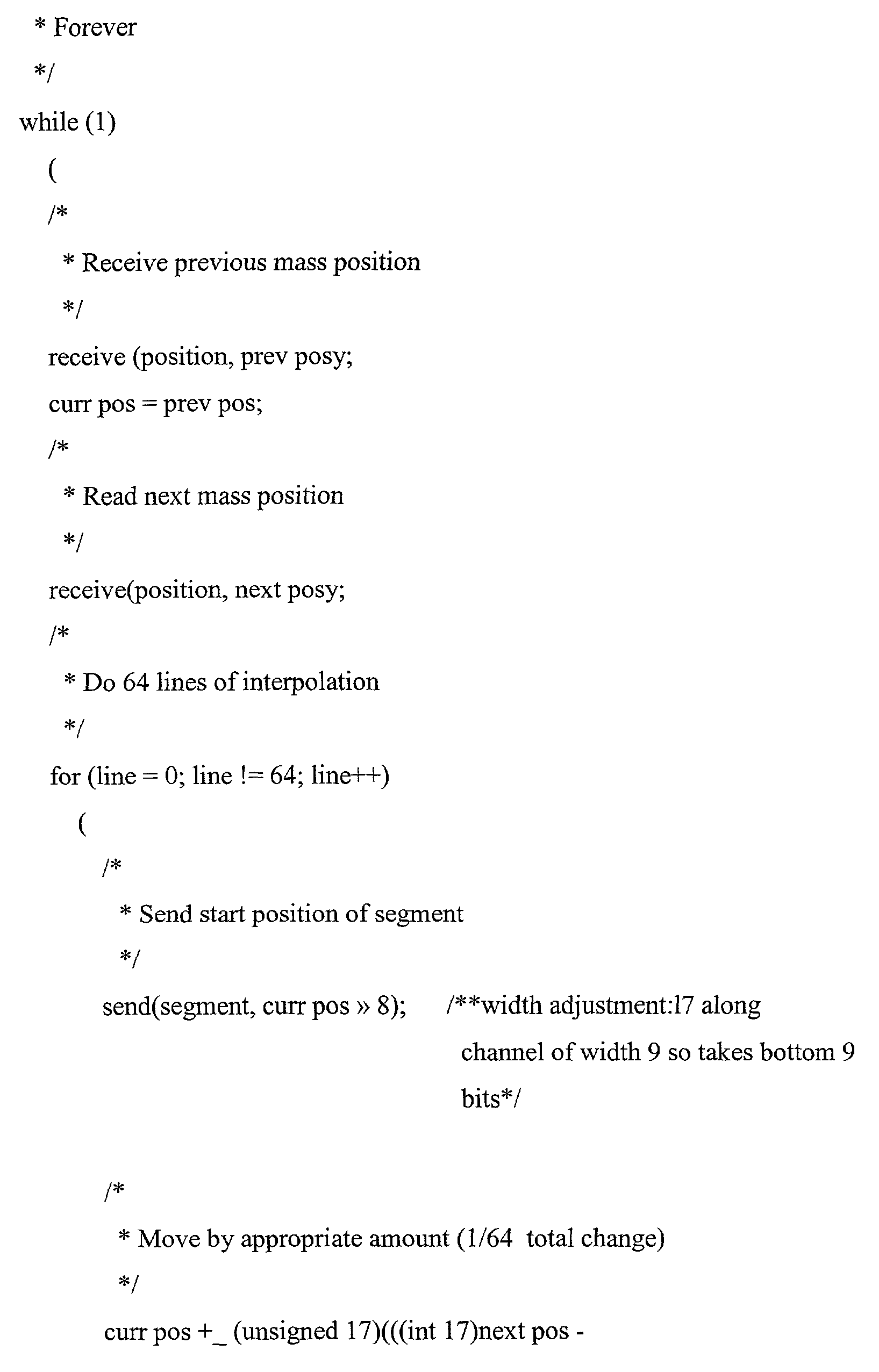


Claims (18)
1. A method for compiling a C function to a reconfigurable logic device, comprising the steps of:
(a) receiving a function written in a C programming language;
(b) compiling the C function into processor instructions;
(c) generating hardware configuration information from the processor instructions; and
(d) utilizing the hardware configuration information for configuring a Field Programmable Gate Array (FPGA) for compiling the function to the FPGA.
2. A method as recited in claim 1 , wherein the function in the FPGA is shared amongst all its uses.
3. A method as recited in claim 1 , wherein the configuration of the FPGA is duplicated for each use.
4. A method as recited in claim 1 , further comprising the step of specifying N copies of the function for use M times.
5. A method as recited in claim 1 , further comprising the step of invoking the function utilizing a token.
6. A method as recited in claim 5 , wherein the step of invoking the function further includes the steps of passing the token to a start signal, routing the start signal and call data to the function, and storing the token in a wait sub-circuit until the function is completed.
7. A computer program product for compiling a C function to a reconfigurable logic device, comprising:
(a) computer code for receiving a function written in a C programming language;
(b) computer code for compiling the C function into processor instructions;
(c) computer code for generating hardware configuration information from the processor instructions; and
(d) computer code for utilizing the hardware configuration information for configuring a Field Programmable Gate Array (FPGA) for compiling the function to the FPGA.
8. A computer program product as recited in claim 7 , wherein the function in the FPGA is shared amongst all its uses.
9. A computer program product as recited in claim 7 , wherein the configuration of the FPGA is duplicated for each use.
10. A computer program product as recited in claim 7 , further comprising computer code for specifying N copies of the function for use M times.
11. A computer program product as recited in claim 7 , further comprising computer code for invoking the function utilizing a token.
12. A computer program product as recited in claim 11 , wherein the computer code for invoking the function further includes computer code for passing the token to a start signal, computer code for routing the start signal and call data to the function, and computer code for storing the token in a wait sub-circuit until the function is completed.
13. A system for compiling a C function to a reconfigurable logic device, comprising:
(a) receiving logic for receiving a function written in a C programming language;
(b) compiling logic for compiling the C function into processor instructions;
(c) conversion logic for generating hardware configuration information from the processor instructions;
(d) a Field Programmable Gate Array (FPGA); and
(e) configuring logic for utilizing the hardware configuration information for configuring the FPGA for compiling the function to the FPGA.
14. A system as recited in claim 13 , wherein the function in the FPGA is shared amongst all its uses.
15. A system as recited in claim 13 , wherein the configuration of the FPGA is duplicated for each use.
16. A system as recited in claim 13 , further comprising logic for specifying N copies of the function for use M times.
17. A system as recited in claim 13 , further comprising control logic for invoking the function utilizing a token.
18. A system as recited in claim 17 , wherein the control logic for invoking the function further includes logic for passing the token to a start signal, logic for routing the start signal and call data to the function, and logic for storing the token in a wait sub-circuit until the function is completed.
Priority Applications (2)
| Application Number | Priority Date | Filing Date | Title |
|---|---|---|---|
| US09/771,963 US20020100029A1 (en) | 2000-07-20 | 2001-01-29 | System, method and article of manufacture for compiling and invoking C functions in hardware |
| PCT/GB2002/000394 WO2002061635A1 (en) | 2001-01-29 | 2002-01-29 | System, method and article of manufacture for compiling and invoking c functions in hardware |
Applications Claiming Priority (3)
| Application Number | Priority Date | Filing Date | Title |
|---|---|---|---|
| US21975400P | 2000-07-20 | 2000-07-20 | |
| US68701100A | 2000-10-12 | 2000-10-12 | |
| US09/771,963 US20020100029A1 (en) | 2000-07-20 | 2001-01-29 | System, method and article of manufacture for compiling and invoking C functions in hardware |
Related Parent Applications (1)
| Application Number | Title | Priority Date | Filing Date |
|---|---|---|---|
| US68701100A Continuation-In-Part | 2000-07-20 | 2000-10-12 |
Publications (1)
| Publication Number | Publication Date |
|---|---|
| US20020100029A1 true US20020100029A1 (en) | 2002-07-25 |
Family
ID=25093472
Family Applications (1)
| Application Number | Title | Priority Date | Filing Date |
|---|---|---|---|
| US09/771,963 Abandoned US20020100029A1 (en) | 2000-07-20 | 2001-01-29 | System, method and article of manufacture for compiling and invoking C functions in hardware |
Country Status (2)
| Country | Link |
|---|---|
| US (1) | US20020100029A1 (en) |
| WO (1) | WO2002061635A1 (en) |
Cited By (49)
| Publication number | Priority date | Publication date | Assignee | Title |
|---|---|---|---|---|
| US20020066088A1 (en) * | 2000-07-03 | 2002-05-30 | Cadence Design Systems, Inc. | System and method for software code optimization |
| US20030120460A1 (en) * | 2001-12-21 | 2003-06-26 | Celoxica Ltd. | System, method, and article of manufacture for enhanced hardware model profiling |
| US20030154466A1 (en) * | 2002-02-11 | 2003-08-14 | Snider Gregory S. | Method and apparatus for compiling source code to configure hardware |
| US20040019883A1 (en) * | 2001-01-26 | 2004-01-29 | Northwestern University | Method and apparatus for automatically generating hardware from algorithms described in matlab |
| US20040109545A1 (en) * | 2002-08-26 | 2004-06-10 | Hardman Clayton M. | Soft chip modem |
| US20050097305A1 (en) * | 2003-10-30 | 2005-05-05 | International Business Machines Corporation | Method and apparatus for using FPGA technology with a microprocessor for reconfigurable, instruction level hardware acceleration |
| US20050132323A1 (en) * | 2003-12-12 | 2005-06-16 | International Business Machines Corporation | Systems and methods for generating applications that are automatically optimized for network performance |
| US20050223388A1 (en) * | 2004-04-01 | 2005-10-06 | Lsi Logic Corporation | System and method for implementing multiple instantiated configurable peripherals in a circuit design |
| US20050229143A1 (en) * | 2004-04-01 | 2005-10-13 | Lsi Logic Corporation | System and method for implementing multiple instantiated configurable peripherals in a circuit design |
| EP1682984A2 (en) * | 2003-11-05 | 2006-07-26 | Stanley M. Hyduke | Method and apparatus for co-verification of digital designs |
| US20070130196A1 (en) * | 2000-12-22 | 2007-06-07 | Star Bridge Systems, Inc. | Removing data set exposers and collectors from behavioral design code |
| US7266487B1 (en) * | 2001-08-29 | 2007-09-04 | Ellipsis Digital Systems, Inc. | Matched instruction set processor systems and method, system, and apparatus to efficiently compile hardware and software designs |
| US20070245326A1 (en) * | 2006-04-12 | 2007-10-18 | Fujitsu Limited | Software/hardware partitioning program and method |
| US20080000111A1 (en) * | 2006-06-29 | 2008-01-03 | Francisco Roberto Green | Excavator control system and method |
| US20080059777A1 (en) * | 2006-08-29 | 2008-03-06 | Jiro Miyake | Semiconductor integrated circuit device and compiler device |
| US20080186052A1 (en) * | 2007-02-01 | 2008-08-07 | International Business Machines Corporation | Methods, systems, and computer program products for using direct memory access to initialize a programmable logic device |
| US20080270331A1 (en) * | 2007-04-26 | 2008-10-30 | Darrin Taylor | Method and system for solving an optimization problem with dynamic constraints |
| US7487507B1 (en) * | 2001-07-18 | 2009-02-03 | City U Research Limited | Secure control transfer in information system |
| US20100228918A1 (en) * | 1999-06-10 | 2010-09-09 | Martin Vorbach | Configurable logic integrated circuit having a multidimensional structure of configurable elements |
| US20100280865A1 (en) * | 2009-04-30 | 2010-11-04 | United Parcel Service Of America, Inc. | Systems and Methods for a Real-Time Workflow Platform |
| US20100281462A1 (en) * | 2009-04-30 | 2010-11-04 | United Parcel Service Of America, Inc. | Systems and methods for generating source code for workflow platform |
| US20110184844A1 (en) * | 2006-06-19 | 2011-07-28 | Exegy Incorporated | High Speed Processing of Financial Information Using FPGA Devices |
| US20120133654A1 (en) * | 2006-09-19 | 2012-05-31 | Caustic Graphics Inc. | Variable-sized concurrent grouping for multiprocessing |
| US8326819B2 (en) | 2006-11-13 | 2012-12-04 | Exegy Incorporated | Method and system for high performance data metatagging and data indexing using coprocessors |
| CN103116493A (en) * | 2013-01-21 | 2013-05-22 | 东南大学 | Automatic mapping method applied to coarsness reconfigurable array |
| US8515682B2 (en) | 2005-03-03 | 2013-08-20 | Washington University | Method and apparatus for performing similarity searching |
| US8620881B2 (en) | 2003-05-23 | 2013-12-31 | Ip Reservoir, Llc | Intelligent data storage and processing using FPGA devices |
| US8762249B2 (en) | 2008-12-15 | 2014-06-24 | Ip Reservoir, Llc | Method and apparatus for high-speed processing of financial market depth data |
| US8843408B2 (en) | 2006-06-19 | 2014-09-23 | Ip Reservoir, Llc | Method and system for high speed options pricing |
| US20140310696A1 (en) * | 2011-06-08 | 2014-10-16 | Hyperion Core Inc. | Tool-level and hardware-level code optimization and respective hardware modification |
| US20150046910A1 (en) * | 2011-12-30 | 2015-02-12 | Intel Corporation | Hardware compilation and/or translation with fault detection and roll back functionality |
| US20150143350A1 (en) * | 2007-08-29 | 2015-05-21 | Convey Computer | Multistate development workflow for generating a custom instruction set reconfigurable processor |
| US20160011982A1 (en) * | 2014-07-14 | 2016-01-14 | Oracle International Corporation | Variable handles |
| US9411918B1 (en) * | 2013-07-24 | 2016-08-09 | Cadence Design Systems, Inc. | Simplified device model extension using subcircuits |
| US9710384B2 (en) | 2008-01-04 | 2017-07-18 | Micron Technology, Inc. | Microprocessor architecture having alternative memory access paths |
| US9735782B1 (en) * | 2016-03-29 | 2017-08-15 | Wipro Limited | Systems and methods for configuring a field programmable device |
| CN107346351A (en) * | 2016-05-06 | 2017-11-14 | 百度(美国)有限责任公司 | For designing FPGA method and system based on the hardware requirement defined in source code |
| US20180046440A1 (en) * | 2015-03-05 | 2018-02-15 | Ingo Josopait | Flow control for language-embedded programming in general purpose computing on graphics processing units |
| US9990393B2 (en) | 2012-03-27 | 2018-06-05 | Ip Reservoir, Llc | Intelligent feed switch |
| US10037568B2 (en) | 2010-12-09 | 2018-07-31 | Ip Reservoir, Llc | Method and apparatus for managing orders in financial markets |
| US10121196B2 (en) | 2012-03-27 | 2018-11-06 | Ip Reservoir, Llc | Offload processing of data packets containing financial market data |
| WO2019002835A1 (en) * | 2017-06-26 | 2019-01-03 | Sony Interactive Entertainment Europe Limited | Data processing |
| US10229453B2 (en) | 2008-01-11 | 2019-03-12 | Ip Reservoir, Llc | Method and system for low latency basket calculation |
| US10430190B2 (en) | 2012-06-07 | 2019-10-01 | Micron Technology, Inc. | Systems and methods for selectively controlling multithreaded execution of executable code segments |
| US10572824B2 (en) | 2003-05-23 | 2020-02-25 | Ip Reservoir, Llc | System and method for low latency multi-functional pipeline with correlation logic and selectively activated/deactivated pipelined data processing engines |
| US10650452B2 (en) | 2012-03-27 | 2020-05-12 | Ip Reservoir, Llc | Offload processing of data packets |
| US10846624B2 (en) | 2016-12-22 | 2020-11-24 | Ip Reservoir, Llc | Method and apparatus for hardware-accelerated machine learning |
| US10909623B2 (en) | 2002-05-21 | 2021-02-02 | Ip Reservoir, Llc | Method and apparatus for processing financial information at hardware speeds using FPGA devices |
| US11436672B2 (en) | 2012-03-27 | 2022-09-06 | Exegy Incorporated | Intelligent switch for processing financial market data |
Family Cites Families (1)
| Publication number | Priority date | Publication date | Assignee | Title |
|---|---|---|---|---|
| US5737631A (en) * | 1995-04-05 | 1998-04-07 | Xilinx Inc | Reprogrammable instruction set accelerator |
-
2001
- 2001-01-29 US US09/771,963 patent/US20020100029A1/en not_active Abandoned
-
2002
- 2002-01-29 WO PCT/GB2002/000394 patent/WO2002061635A1/en not_active Application Discontinuation
Cited By (113)
| Publication number | Priority date | Publication date | Assignee | Title |
|---|---|---|---|---|
| US8726250B2 (en) * | 1999-06-10 | 2014-05-13 | Pact Xpp Technologies Ag | Configurable logic integrated circuit having a multidimensional structure of configurable elements |
| US20100228918A1 (en) * | 1999-06-10 | 2010-09-09 | Martin Vorbach | Configurable logic integrated circuit having a multidimensional structure of configurable elements |
| US20020066088A1 (en) * | 2000-07-03 | 2002-05-30 | Cadence Design Systems, Inc. | System and method for software code optimization |
| US20070130196A1 (en) * | 2000-12-22 | 2007-06-07 | Star Bridge Systems, Inc. | Removing data set exposers and collectors from behavioral design code |
| US20040019883A1 (en) * | 2001-01-26 | 2004-01-29 | Northwestern University | Method and apparatus for automatically generating hardware from algorithms described in matlab |
| US7000213B2 (en) * | 2001-01-26 | 2006-02-14 | Northwestern University | Method and apparatus for automatically generating hardware from algorithms described in MATLAB |
| US7487507B1 (en) * | 2001-07-18 | 2009-02-03 | City U Research Limited | Secure control transfer in information system |
| US7266487B1 (en) * | 2001-08-29 | 2007-09-04 | Ellipsis Digital Systems, Inc. | Matched instruction set processor systems and method, system, and apparatus to efficiently compile hardware and software designs |
| US20030120460A1 (en) * | 2001-12-21 | 2003-06-26 | Celoxica Ltd. | System, method, and article of manufacture for enhanced hardware model profiling |
| US20030154466A1 (en) * | 2002-02-11 | 2003-08-14 | Snider Gregory S. | Method and apparatus for compiling source code to configure hardware |
| US6988192B2 (en) * | 2002-02-11 | 2006-01-17 | Hewlett-Packard Development Company, L.P. | Method and apparatus for compiling source code to configure hardware |
| US10909623B2 (en) | 2002-05-21 | 2021-02-02 | Ip Reservoir, Llc | Method and apparatus for processing financial information at hardware speeds using FPGA devices |
| US7970044B2 (en) * | 2002-08-26 | 2011-06-28 | Hardman Clayton M | Soft chip modem |
| US20040109545A1 (en) * | 2002-08-26 | 2004-06-10 | Hardman Clayton M. | Soft chip modem |
| US9898312B2 (en) | 2003-05-23 | 2018-02-20 | Ip Reservoir, Llc | Intelligent data storage and processing using FPGA devices |
| US10719334B2 (en) | 2003-05-23 | 2020-07-21 | Ip Reservoir, Llc | Intelligent data storage and processing using FPGA devices |
| US8751452B2 (en) | 2003-05-23 | 2014-06-10 | Ip Reservoir, Llc | Intelligent data storage and processing using FPGA devices |
| US10929152B2 (en) | 2003-05-23 | 2021-02-23 | Ip Reservoir, Llc | Intelligent data storage and processing using FPGA devices |
| US10572824B2 (en) | 2003-05-23 | 2020-02-25 | Ip Reservoir, Llc | System and method for low latency multi-functional pipeline with correlation logic and selectively activated/deactivated pipelined data processing engines |
| US8768888B2 (en) | 2003-05-23 | 2014-07-01 | Ip Reservoir, Llc | Intelligent data storage and processing using FPGA devices |
| US11275594B2 (en) | 2003-05-23 | 2022-03-15 | Ip Reservoir, Llc | Intelligent data storage and processing using FPGA devices |
| US9176775B2 (en) | 2003-05-23 | 2015-11-03 | Ip Reservoir, Llc | Intelligent data storage and processing using FPGA devices |
| US10346181B2 (en) | 2003-05-23 | 2019-07-09 | Ip Reservoir, Llc | Intelligent data storage and processing using FPGA devices |
| US8620881B2 (en) | 2003-05-23 | 2013-12-31 | Ip Reservoir, Llc | Intelligent data storage and processing using FPGA devices |
| US20050097305A1 (en) * | 2003-10-30 | 2005-05-05 | International Business Machines Corporation | Method and apparatus for using FPGA technology with a microprocessor for reconfigurable, instruction level hardware acceleration |
| US7584345B2 (en) | 2003-10-30 | 2009-09-01 | International Business Machines Corporation | System for using FPGA technology with a microprocessor for reconfigurable, instruction level hardware acceleration |
| US7603540B2 (en) | 2003-10-30 | 2009-10-13 | International Business Machines Corporation | Using field programmable gate array (FPGA) technology with a microprocessor for reconfigurable, instruction level hardware acceleration |
| EP1682984A2 (en) * | 2003-11-05 | 2006-07-26 | Stanley M. Hyduke | Method and apparatus for co-verification of digital designs |
| EP1682984A4 (en) * | 2003-11-05 | 2008-03-12 | Stanley M Hyduke | Method and apparatus for co-verification of digital designs |
| US20050132323A1 (en) * | 2003-12-12 | 2005-06-16 | International Business Machines Corporation | Systems and methods for generating applications that are automatically optimized for network performance |
| US7437707B2 (en) * | 2003-12-12 | 2008-10-14 | International Business Machines Corporation | Systems and methods for generating applications that are automatically optimized for network performance |
| US20050223388A1 (en) * | 2004-04-01 | 2005-10-06 | Lsi Logic Corporation | System and method for implementing multiple instantiated configurable peripherals in a circuit design |
| US7620743B2 (en) * | 2004-04-01 | 2009-11-17 | Lsi Corporation | System and method for implementing multiple instantiated configurable peripherals in a circuit design |
| US20050229143A1 (en) * | 2004-04-01 | 2005-10-13 | Lsi Logic Corporation | System and method for implementing multiple instantiated configurable peripherals in a circuit design |
| US10957423B2 (en) | 2005-03-03 | 2021-03-23 | Washington University | Method and apparatus for performing similarity searching |
| US9547680B2 (en) | 2005-03-03 | 2017-01-17 | Washington University | Method and apparatus for performing similarity searching |
| US8515682B2 (en) | 2005-03-03 | 2013-08-20 | Washington University | Method and apparatus for performing similarity searching |
| US10580518B2 (en) | 2005-03-03 | 2020-03-03 | Washington University | Method and apparatus for performing similarity searching |
| US20070245326A1 (en) * | 2006-04-12 | 2007-10-18 | Fujitsu Limited | Software/hardware partitioning program and method |
| US7908592B2 (en) * | 2006-04-12 | 2011-03-15 | Fujitsu Semiconductor Limited | Software/hardware partitioning program and method |
| US10360632B2 (en) | 2006-06-19 | 2019-07-23 | Ip Reservoir, Llc | Fast track routing of streaming data using FPGA devices |
| US9916622B2 (en) | 2006-06-19 | 2018-03-13 | Ip Reservoir, Llc | High speed processing of financial information using FPGA devices |
| US10817945B2 (en) | 2006-06-19 | 2020-10-27 | Ip Reservoir, Llc | System and method for routing of streaming data as between multiple compute resources |
| US8595104B2 (en) | 2006-06-19 | 2013-11-26 | Ip Reservoir, Llc | High speed processing of financial information using FPGA devices |
| US8600856B2 (en) | 2006-06-19 | 2013-12-03 | Ip Reservoir, Llc | High speed processing of financial information using FPGA devices |
| US8478680B2 (en) | 2006-06-19 | 2013-07-02 | Exegy Incorporated | High speed processing of financial information using FPGA devices |
| US8626624B2 (en) | 2006-06-19 | 2014-01-07 | Ip Reservoir, Llc | High speed processing of financial information using FPGA devices |
| US8655764B2 (en) | 2006-06-19 | 2014-02-18 | Ip Reservoir, Llc | High speed processing of financial information using FPGA devices |
| US8458081B2 (en) | 2006-06-19 | 2013-06-04 | Exegy Incorporated | High speed processing of financial information using FPGA devices |
| US9672565B2 (en) | 2006-06-19 | 2017-06-06 | Ip Reservoir, Llc | High speed processing of financial information using FPGA devices |
| US20110184844A1 (en) * | 2006-06-19 | 2011-07-28 | Exegy Incorporated | High Speed Processing of Financial Information Using FPGA Devices |
| US9582831B2 (en) | 2006-06-19 | 2017-02-28 | Ip Reservoir, Llc | High speed processing of financial information using FPGA devices |
| US10504184B2 (en) | 2006-06-19 | 2019-12-10 | Ip Reservoir, Llc | Fast track routing of streaming data as between multiple compute resources |
| US10467692B2 (en) | 2006-06-19 | 2019-11-05 | Ip Reservoir, Llc | High speed processing of financial information using FPGA devices |
| US8843408B2 (en) | 2006-06-19 | 2014-09-23 | Ip Reservoir, Llc | Method and system for high speed options pricing |
| US10169814B2 (en) | 2006-06-19 | 2019-01-01 | Ip Reservoir, Llc | High speed processing of financial information using FPGA devices |
| US11182856B2 (en) | 2006-06-19 | 2021-11-23 | Exegy Incorporated | System and method for routing of streaming data as between multiple compute resources |
| US8407122B2 (en) | 2006-06-19 | 2013-03-26 | Exegy Incorporated | High speed processing of financial information using FPGA devices |
| US20080000111A1 (en) * | 2006-06-29 | 2008-01-03 | Francisco Roberto Green | Excavator control system and method |
| US20080059777A1 (en) * | 2006-08-29 | 2008-03-06 | Jiro Miyake | Semiconductor integrated circuit device and compiler device |
| US9665970B2 (en) * | 2006-09-19 | 2017-05-30 | Imagination Technologies Limited | Variable-sized concurrent grouping for multiprocessing |
| US20120133654A1 (en) * | 2006-09-19 | 2012-05-31 | Caustic Graphics Inc. | Variable-sized concurrent grouping for multiprocessing |
| US9323794B2 (en) | 2006-11-13 | 2016-04-26 | Ip Reservoir, Llc | Method and system for high performance pattern indexing |
| US8326819B2 (en) | 2006-11-13 | 2012-12-04 | Exegy Incorporated | Method and system for high performance data metatagging and data indexing using coprocessors |
| US8495545B2 (en) | 2007-02-01 | 2013-07-23 | International Business Machines Corporation | Using direct memory access to initialize a programmable logic device |
| US20080186052A1 (en) * | 2007-02-01 | 2008-08-07 | International Business Machines Corporation | Methods, systems, and computer program products for using direct memory access to initialize a programmable logic device |
| US8589834B2 (en) | 2007-02-01 | 2013-11-19 | International Business Machines Corporation | Using direct memory access to initialize a programmable logic device |
| US8407658B2 (en) | 2007-02-01 | 2013-03-26 | International Business Machines Corporation | Methods, systems, and computer program products for using direct memory access to initialize a programmable logic device |
| US8069127B2 (en) | 2007-04-26 | 2011-11-29 | 21 Ct, Inc. | Method and system for solving an optimization problem with dynamic constraints |
| US20080270331A1 (en) * | 2007-04-26 | 2008-10-30 | Darrin Taylor | Method and system for solving an optimization problem with dynamic constraints |
| US20150143350A1 (en) * | 2007-08-29 | 2015-05-21 | Convey Computer | Multistate development workflow for generating a custom instruction set reconfigurable processor |
| US10223081B2 (en) * | 2007-08-29 | 2019-03-05 | Micron Technology, Inc. | Multistate development workflow for generating a custom instruction set reconfigurable processor |
| US11106592B2 (en) | 2008-01-04 | 2021-08-31 | Micron Technology, Inc. | Microprocessor architecture having alternative memory access paths |
| US9710384B2 (en) | 2008-01-04 | 2017-07-18 | Micron Technology, Inc. | Microprocessor architecture having alternative memory access paths |
| US10229453B2 (en) | 2008-01-11 | 2019-03-12 | Ip Reservoir, Llc | Method and system for low latency basket calculation |
| US10929930B2 (en) | 2008-12-15 | 2021-02-23 | Ip Reservoir, Llc | Method and apparatus for high-speed processing of financial market depth data |
| US8768805B2 (en) | 2008-12-15 | 2014-07-01 | Ip Reservoir, Llc | Method and apparatus for high-speed processing of financial market depth data |
| US8762249B2 (en) | 2008-12-15 | 2014-06-24 | Ip Reservoir, Llc | Method and apparatus for high-speed processing of financial market depth data |
| US10062115B2 (en) | 2008-12-15 | 2018-08-28 | Ip Reservoir, Llc | Method and apparatus for high-speed processing of financial market depth data |
| US11676206B2 (en) | 2008-12-15 | 2023-06-13 | Exegy Incorporated | Method and apparatus for high-speed processing of financial market depth data |
| US8332811B2 (en) | 2009-04-30 | 2012-12-11 | United Parcel Service Of America, Inc. | Systems and methods for generating source code for workflow platform |
| US20100281462A1 (en) * | 2009-04-30 | 2010-11-04 | United Parcel Service Of America, Inc. | Systems and methods for generating source code for workflow platform |
| US9911092B2 (en) | 2009-04-30 | 2018-03-06 | United Parcel Service Of America, Inc. | Systems and methods for a real-time workflow platform |
| US10713608B2 (en) | 2009-04-30 | 2020-07-14 | United Parcel Service Of America, Inc. | Systems and methods for a real-time workflow platform |
| US20100280865A1 (en) * | 2009-04-30 | 2010-11-04 | United Parcel Service Of America, Inc. | Systems and Methods for a Real-Time Workflow Platform |
| US8751284B2 (en) | 2009-04-30 | 2014-06-10 | United Parcel Service Of America, Inc. | Systems and methods for a real-time workflow platform using Petri net model mappings |
| US10037568B2 (en) | 2010-12-09 | 2018-07-31 | Ip Reservoir, Llc | Method and apparatus for managing orders in financial markets |
| US11803912B2 (en) | 2010-12-09 | 2023-10-31 | Exegy Incorporated | Method and apparatus for managing orders in financial markets |
| US11397985B2 (en) | 2010-12-09 | 2022-07-26 | Exegy Incorporated | Method and apparatus for managing orders in financial markets |
| US9703538B2 (en) * | 2011-06-08 | 2017-07-11 | Hyperion Core, Inc. | Tool-level and hardware-level code optimization and respective hardware modification |
| US20140310696A1 (en) * | 2011-06-08 | 2014-10-16 | Hyperion Core Inc. | Tool-level and hardware-level code optimization and respective hardware modification |
| US20150046910A1 (en) * | 2011-12-30 | 2015-02-12 | Intel Corporation | Hardware compilation and/or translation with fault detection and roll back functionality |
| US9317263B2 (en) * | 2011-12-30 | 2016-04-19 | Intel Corporation | Hardware compilation and/or translation with fault detection and roll back functionality |
| US10650452B2 (en) | 2012-03-27 | 2020-05-12 | Ip Reservoir, Llc | Offload processing of data packets |
| US9990393B2 (en) | 2012-03-27 | 2018-06-05 | Ip Reservoir, Llc | Intelligent feed switch |
| US11436672B2 (en) | 2012-03-27 | 2022-09-06 | Exegy Incorporated | Intelligent switch for processing financial market data |
| US10121196B2 (en) | 2012-03-27 | 2018-11-06 | Ip Reservoir, Llc | Offload processing of data packets containing financial market data |
| US10963962B2 (en) | 2012-03-27 | 2021-03-30 | Ip Reservoir, Llc | Offload processing of data packets containing financial market data |
| US10872078B2 (en) | 2012-03-27 | 2020-12-22 | Ip Reservoir, Llc | Intelligent feed switch |
| US10430190B2 (en) | 2012-06-07 | 2019-10-01 | Micron Technology, Inc. | Systems and methods for selectively controlling multithreaded execution of executable code segments |
| US10534591B2 (en) | 2012-10-23 | 2020-01-14 | Micron Technology, Inc. | Multistage development workflow for generating a custom instruction set reconfigurable processor |
| CN103116493A (en) * | 2013-01-21 | 2013-05-22 | 东南大学 | Automatic mapping method applied to coarsness reconfigurable array |
| US9411918B1 (en) * | 2013-07-24 | 2016-08-09 | Cadence Design Systems, Inc. | Simplified device model extension using subcircuits |
| US9690709B2 (en) * | 2014-07-14 | 2017-06-27 | Oracle International Corporation | Variable handles |
| US11030105B2 (en) | 2014-07-14 | 2021-06-08 | Oracle International Corporation | Variable handles |
| US20160011982A1 (en) * | 2014-07-14 | 2016-01-14 | Oracle International Corporation | Variable handles |
| US20180046440A1 (en) * | 2015-03-05 | 2018-02-15 | Ingo Josopait | Flow control for language-embedded programming in general purpose computing on graphics processing units |
| US10459702B2 (en) * | 2015-03-05 | 2019-10-29 | Ingo Josopait | Flow control for language-embedded programming in general purpose computing on graphics processing units |
| US9735782B1 (en) * | 2016-03-29 | 2017-08-15 | Wipro Limited | Systems and methods for configuring a field programmable device |
| CN107346351A (en) * | 2016-05-06 | 2017-11-14 | 百度(美国)有限责任公司 | For designing FPGA method and system based on the hardware requirement defined in source code |
| US11416778B2 (en) | 2016-12-22 | 2022-08-16 | Ip Reservoir, Llc | Method and apparatus for hardware-accelerated machine learning |
| US10846624B2 (en) | 2016-12-22 | 2020-11-24 | Ip Reservoir, Llc | Method and apparatus for hardware-accelerated machine learning |
| WO2019002835A1 (en) * | 2017-06-26 | 2019-01-03 | Sony Interactive Entertainment Europe Limited | Data processing |
Also Published As
| Publication number | Publication date |
|---|---|
| WO2002061635A1 (en) | 2002-08-08 |
Similar Documents
| Publication | Publication Date | Title |
|---|---|---|
| US20020100029A1 (en) | System, method and article of manufacture for compiling and invoking C functions in hardware | |
| US20030121010A1 (en) | System, method, and article of manufacture for estimating a potential performance of a codesign from an executable specification | |
| US20030140337A1 (en) | System, method, and article of manufacture for data transfer reporting for an application | |
| US20030117971A1 (en) | System, method, and article of manufacture for profiling an executable hardware model using calls to profiling functions | |
| US20020072893A1 (en) | System, method and article of manufacture for using a microprocessor emulation in a hardware application with non time-critical functions | |
| US6668312B2 (en) | System, method, and article of manufacture for dynamically profiling memory transfers in a program | |
| Koch et al. | FPGAs for software programmers | |
| US20030120460A1 (en) | System, method, and article of manufacture for enhanced hardware model profiling | |
| Chou et al. | The chinook hardware/software co-synthesis system | |
| De Micheli | Computer-aided hardware-software codesign | |
| EP1004085B1 (en) | System and method for converting graphical programs into hardware implementations | |
| WO2000038087A1 (en) | Hardware/software codesign system | |
| Jantsch et al. | Models of computation and languages for embedded system design | |
| Thomas et al. | Industrial uses of the system architect’s workbench | |
| US7475000B2 (en) | Apparatus and method for managing integrated circuit designs | |
| US6053947A (en) | Simulation model using object-oriented programming | |
| US20030023653A1 (en) | System, method and article of manufacture for a single-cycle floating point library | |
| Quadri | MARTE based model driven design methodology for targeting dynamically reconfigurable FPGA based SoCs | |
| Meredith | High-level SystemC synthesis with forte's cynthesizer | |
| Ortega et al. | Models and methods for hw/sw intellectual property interfacing | |
| Saul | Hardware/software codesign for FPGA-based systems | |
| Cesario et al. | Object-based hardware/software component interconnection model for interface design in system-on-a-chip circuits | |
| WO2002031647A2 (en) | System, method and article of manufacture for using a microprocessor emulation in a hardware application with non time-critical functions | |
| WO2002031678A2 (en) | System and method for an operating system in a reconfigurable logic device | |
| Dutt et al. | Exel: A language for interactive behavioral synthesis |
Legal Events
| Date | Code | Title | Description |
|---|---|---|---|
| AS | Assignment |
Owner name: CELOXICA LTD, UNITED KINGDOM Free format text: ASSIGNMENT OF ASSIGNORS INTEREST;ASSIGNOR:BOWEN, MATT;REEL/FRAME:011838/0054 Effective date: 20010517 |
|
| STCB | Information on status: application discontinuation |
Free format text: EXPRESSLY ABANDONED -- DURING EXAMINATION |