US6292874B1 - Memory management method and apparatus for partitioning homogeneous memory and restricting access of installed applications to predetermined memory ranges - Google Patents
Memory management method and apparatus for partitioning homogeneous memory and restricting access of installed applications to predetermined memory ranges Download PDFInfo
- Publication number
- US6292874B1 US6292874B1 US09/420,318 US42031899A US6292874B1 US 6292874 B1 US6292874 B1 US 6292874B1 US 42031899 A US42031899 A US 42031899A US 6292874 B1 US6292874 B1 US 6292874B1
- Authority
- US
- United States
- Prior art keywords
- memory
- management unit
- volatile
- application
- processing circuit
- Prior art date
- Legal status (The legal status is an assumption and is not a legal conclusion. Google has not performed a legal analysis and makes no representation as to the accuracy of the status listed.)
- Expired - Lifetime
Links
Images


Classifications
-
- G—PHYSICS
- G06—COMPUTING; CALCULATING OR COUNTING
- G06F—ELECTRIC DIGITAL DATA PROCESSING
- G06F12/00—Accessing, addressing or allocating within memory systems or architectures
- G06F12/02—Addressing or allocation; Relocation
-
- G—PHYSICS
- G06—COMPUTING; CALCULATING OR COUNTING
- G06F—ELECTRIC DIGITAL DATA PROCESSING
- G06F12/00—Accessing, addressing or allocating within memory systems or architectures
- G06F12/14—Protection against unauthorised use of memory or access to memory
- G06F12/1416—Protection against unauthorised use of memory or access to memory by checking the object accessibility, e.g. type of access defined by the memory independently of subject rights
- G06F12/145—Protection against unauthorised use of memory or access to memory by checking the object accessibility, e.g. type of access defined by the memory independently of subject rights the protection being virtual, e.g. for virtual blocks or segments before a translation mechanism
Definitions
- the present invention relates generally to a memory management system for single-chip data processing circuits, such as a smart card, and more particularly, to a memory management method and apparatus that (i) partitions homogeneous memory devices to achieve heterogeneous memory characteristics and (ii) restricts access of installed applications to predetermined memory ranges.
- Smart cards typically contain a central processing unit (CPU) or a microprocessor to control all processes and transactions associated with the smart card.
- the microprocessor is used to increase the security of the device, by providing a flexible method to implement complex and variable algorithms that ensure integrity and access to data stored in non volatile memory.
- smart cards contain non-volatile memory, for storing program code and changed data, and volatile memory for the temporary storage of certain information. In conventional smart cards, each memory type has been implemented using different technologies.
- Byte erasable EEPROM for example, is typically used to store non-volatile data, that changes or configures the device in the field, while Masked-Rom and more recently one-time-programmable read-only memory (OTPROM) is typically used to store program code.
- OTPROM one-time-programmable read-only memory
- Volatile memory is normally implemented as random access memory (RAM).
- RAM random access memory
- the hardware technologies associated with each memory type provide desirable security benefits. For example, the one-time nature of OTPROM prevents authorized program code from being modified or over-written with unauthorized program code. Likewise, the implementation of volatile memory as RAM ensures that the temporarily stored information, such as an encryption key, is cleared after each use.
- FERAM ferroelectric random access memory
- FERAM ferroelectric random access memory
- Such homogeneous memory devices are desirable since they are non-volatile, while providing the speed of RAM, and the density of ROM while using little energy.
- the homogeneous nature of such memory devices eliminates the security benefits that were previously provided by the various hardware technologies themselves. Thus, a need exists for the ability to partition such otherwise homogeneous memory devices into volatile, non-volatile and program storage (ROM) regions with the appropriate corresponding memory characteristics.
- U.S. Pat. No. 5,890,199 to Downs discloses a system for selectively configuring a homogeneous memory, such as FERAM, as read/write memory, read only memory (ROM) or a combination of the foregoing.
- a homogeneous memory such as FERAM
- ROM read only memory
- the Downs system allows a single portion of the memory array to be partitioned as ROM for storing the software code for only an application.
- the Downs system does not provide a mechanism for configuring the homogeneous memory to behave like RAM that provides for the temporary storage of information that is cleared after each use.
- Single-chip microprocessors such as those used in smart cards, increasingly support multiple functions (applications) and must be able to download an application for immediate execution in support of a given function.
- a system would allow a third party to create an application and load it onto a standard card, which removes the control over the integrity of the software allowing malicious attacks.
- This may be overcome, for example, by programming an interpreter into the card that indirectly executes a command sequence (as opposed to the microprocessor executing a binary directly).
- This technique requires more processing power for a given function and additional code on the device which further increases the cost of a cost-sensitive product.
- a mechanism is required that ensures that every memory transaction made by a loaded application is limited to the memory areas allocated to it. Furthermore, this mechanism needs to function independently of the software such that it cannot be altered by malicious programs. Thus, even malicious software is controlled.
- Hardware-implementations of an access control mechanism will maximize the security of the single-chip microprocessor, and allow code to be reused, by isolating the code from the actual hardware implementation of the device.
- a hardware-implemented access control mechanism allows a secure kernel (operating system) to be embedded into the device, having access rights to features of the device that are denied to applications.
- a memory management unit for a single-chip data processing circuit, such as a smart card.
- the memory management unit (i) partitions a homogeneous memory device to achieve heterogeneous memory characteristics for various regions of the memory device, and (ii) restricts access of installed applications executing in the microprocessor core to predetermined memory ranges.
- the memory management unit imposes firewalls between applications and permits hardware checked partitioning of the memory.
- the memory management unit provides two operating modes for the processing circuit.
- a secure kernel mode the programmer can access all resources of the device including hardware control.
- an application mode the memory management unit translates the virtual memory address used by the software creator into the physical address allocated to the application by the operating system in a secure kernel mode during installation.
- the present invention also ensures that an application does not access memory outside of the memory mapped to the application by the software when in secure kernel mode. Any illegal memory accesses attempted by an application will cause a trap, and in one embodiment, the memory management unit restarts the microprocessor in a secure kernel mode, optionally setting flags to permit a system programmer to implement an appropriate mechanism to deal with the exception.
- An application table records the memory demands of each application that is installed on the single-chip data processing circuit, such as the volatile, non-volatile and program storage (OTPROM) memory requirements of each application.
- the memory management unit implements memory address checking using limit registers and translates virtual addresses to an absolute memory address using offset registers. Once the appropriate memory areas have been allocated to each application program, the memory management unit loads limit and offset registers with the appropriate values from the application table to ensure that the executing application only accesses the designated memory locations.
- the memory management unit partitions a homogeneous memory device, such as an FERAM memory device, to achieve heterogeneous memory characteristics normally associated with a plurality of memory technologies, such as volatile, non-volatile and program storage (ROM) memory segments.
- a homogeneous memory device such as an FERAM memory device
- ROM volatile, non-volatile and program storage
- the memory management unit enforces the appropriate corresponding memory characteristics for each heterogeneous memory type.
- a memory partition control logic is programmed with the required partitioning associated with each portion of the homogeneous memory in order that the homogeneous memory behaves like volatile, non-volatile and program storage (OTPROM) memory technologies, as desired.
- FIG. 1 is a schematic block diagram illustrating a single-chip data processing circuit, such as a smart card, that includes a memory management unit in accordance with the present invention
- FIG. 2 is a schematic block diagram of an exemplary hardware-implementation of the memory management unit of FIG. 1;
- FIG. 3 is a sample table from the exemplary application table of FIG. 2;
- FIG. 4 is a schematic block diagram illustrating the memory partition control logic of FIG. 2 .
- FIG. 1 illustrates a single-chip data processing circuit 100 , such as a smart card, that includes a microprocessor core 110 , memory devices 120 , 130 and a memory management unit 200 that interfaces between the microprocessor core 110 and the memory devices 120 , 130 for memory access operations.
- the memory management unit 200 (i) partitions a homogeneous memory device to achieve heterogeneous memory characteristics for various regions of the memory device, and (ii) restricts access of installed applications executing in the microprocessor core 110 to predetermined memory ranges. It is noted that each of these two features are independent, and may be selectively and separately implemented in the memory management unit 200 , as would be apparent to a person of ordinary skill.
- the present invention is illustrated in a smart card environment, the present invention applies to any single-chip data processing circuit, as would be apparent to a person of ordinary skill in the art.
- the memory management unit 200 imposes firewalls between applications and thereby permits hardware checked partitioning of the memory. Thus, an application has limited access to only a predetermined memory range. As discussed further below, the memory management unit 200 performs memory address checking and translates addresses based on user-specified criteria.
- the memory management unit 200 provides two operating modes for the microprocessor 110 .
- a secure kernel mode the programmer can access all resources of the device including hardware control.
- an application mode the memory management unit 200 translates the virtual memory address used by the software creator into the physical address allocated to the application by the operating system in a secure kernel mode during installation.
- the present invention also ensures that an application does not access memory outside of the memory mapped to the application by the software when in secure kernel mode. Any illegal memory accesses attempted by an application will cause a trap, and in one embodiment, the memory management unit 200 restarts the microprocessor 10 in a secure kernel mode, optionally setting flags to permit a system programmer to implement an appropriate mechanism to deal with the exception.
- an exception is identified if an application is written with the accidental or specific intention of compromising the security of the smart card, by accessing stored data, code or by manipulating the hardware to indirectly influence the operation of the chip.
- the memory management unit 200 limits the application to the allocated program code and data areas. Any other references result in termination of the application and flagging the secure kernel that such an illegal attempt has been made.
- each application is isolated from all other applications, the hardware and the secure kernel.
- the security mechanism acts as a general protection unit trapping software errors.
- the memory management unit 200 partitions a homogeneous memory device, such as an FERAM memory device, to achieve heterogeneous memory characteristics normally associated with a plurality of memory technologies, such as volatile, non-volatile and program storage (ROM) memory segments. Once partitioned, the memory management unit 200 enforces the appropriate corresponding memory characteristics for each heterogeneous memory type.
- a homogeneous memory device such as an FERAM memory device
- ROM program storage
- FIG. 2 provides a schematic block diagram of an exemplary hardware-implementation of the memory management unit 200 .
- the memory management unit 200 (i) partitions a homogeneous memory device to achieve heterogeneous memory characteristics for various regions of the memory device, and (ii) restricts access of installed applications executing in the microprocessor core 110 to predetermined memory ranges.
- the memory management unit 200 includes a section for memory partition control logic 400 .
- the memory partition control logic 400 is programmed with the required partitioning associated with each portion of the homogeneous memory in order that the homogeneous memory behaves like volatile, non-volatile and program storage (OTPROM) memory technologies, as desired.
- OTPROM volatile, non-volatile and program storage
- An application would normally be allocated different memory areas for code and data, and the data area can be further divided into a volatile portion, for scratch pad operations, and non-volatile storage areas.
- the memory management unit 200 includes an application table 300 , discussed further below in conjunction with FIG. 3 .
- the application table 300 records the memory demands of each application that is installed on the single-chip data processing circuit 100 .
- the application table 300 indicates the volatile, non-volatile and program storage (OTPROM) memory requirements of each application.
- OTPROM volatile, non-volatile and program storage
- the application table 300 is generated by the microprocessor 110 when operating in a secure kernel mode, as each application is installed. The kernel allocates the appropriate memory areas to each application program.
- the memory management unit 200 shown in FIG. 2 can load the limit and offset registers 230 - 232 , 240 - 242 , discussed below, with the appropriate values from the application table 300 to ensure that the executing application only accesses the designated memory locations.
- the memory management unit 200 implements memory address checking using the limit registers 230 - 232 and translates addresses to an absolute memory address using the offset registers 240 - 242 .
- the memory management unit 200 In addition to restricting access of installed applications executing in the microprocessor core 110 to predetermined memory ranges, the memory management unit 200 also translates addresses between the virtual memory address used by the software programmer into the physical address allocated to the application by the operating system in a secure kernel mode, before it hands over execution to the application code. It is noted that when programming the illustrative 8051 microprocessor, a software programmer starts with a code space starting at an address of 0, and a data space starting at an address of 0. Furthermore, the size of the code and data space is a variable corresponding to the required resource of a given application.
- the application has the appropriate volatile, non-volatile and program storage (OTPROM) memory allocations that are translated and checked by the memory management unit 200 , in a manner described below, such that attempts to access memory outside the designated memory area will result in the application being terminated.
- OTPROM volatile, non-volatile and program storage
- the hardware memory-mapping scheme and out of area protection hardware mechanism is shown in FIG. 2 .
- the microprocessor core 110 must implement context switching in a multi-function environment, as would be apparent to a person of ordinary skill.
- the memory management unit 200 includes a pair of limit and offset registers, such as the registers 230 - 232 , 240 - 242 , respectively, for each memory technology that is managed by the memory management unit 200 .
- the associated memory requirements are retrieved from the application table 300 by the secure operating system running in the kernel mode.
- the associated memory requirements are loaded into the corresponding limit and offset registers 230 - 232 , 240 - 242 .
- the kernel loads the code application offset register (COR) 240 with the address of where the application program code is stored in memory.
- the kernel then loads the code application limit register (CLR) 230 with the size of the application code space.
- the data space can be defined as a block of memory, whose size is the sum of the sizes of both the volatile and non-volatile memory, allocated to that application.
- the kernel loads the data limit register (DLR) 231 with the size of the data space (both the volatile and nonvolatile memory).
- the size of the allocated volatile memory is loaded into the volatile data limit register (VDLR) 232 , and the base address to be used for the scratch pad memory (RAM) is loaded into the volatile data offset register (VDOR) 241 .
- the base address to be used for non-volatile storage (EEPROM) allocated to the application is loaded into the non volatile offset register (NVOR) 242 .
- the memory protection mechanism checks the virtual memory addresses assigned by the programmer, as opposed to the absolute addresses allocated by the kernel.
- the illegal access mechanism is simplified, as an illegal memory access is identified when an access is made to a location having a virtual address that is greater than the value contained in the appropriate limit register.
- the memory management unit 200 contains comparators 250 , 255 for comparing the virtual address issued by the microprocessor core 210 , to the value contained in the appropriate limit register 230 - 232 . If the application is attempting an unauthorized memory access, the corresponding comparator 250 , 255 will set an out-of-bounds trap.
- the corresponding comparator 250 , 255 will enable the appropriate offset register 240 - 242 , and the value from the offset register will be added by an adder 260 to the virtual address issued by the microprocessor core 210 .
- the limit and offset registers 230 - 232 , 240 - 242 and the comparators 250 , 255 are fabricated using known tamper-resistant technologies to preclude physical security attack.
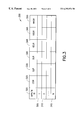
- FIG. 3 illustrates an exemplary application table 300 that stores information on each application installed on the single-chip data processing circuit 100 , including the memory demands of each installed application.
- the application table 300 indicates the volatile, non-volatile and program storage (OTPROM) memory requirements of each application.
- OTPROM program storage
- the application table 300 may be generated by the microprocessor 110 when operating in a secure kernel mode, as each application is installed. The kernel allocates the appropriate memory areas to each application program.
- the application table 300 maintains a plurality of records, such as records 305 - 315 , each associated with a different application. For each application identifier in field 320 , the application table 300 includes the base address of where the application program code is stored in memory, and the corresponding size of the application code space in fields 325 and 330 , respectively. In addition, the application table 300 indicates the total size of the data space in field 335 (sum of both the volatile and non-volatile memory), with the size of the allocated volatile memory stored in field 340 , the base address for the scratch pad memory (RAM) in field 345 , and the base address for non-volatile storage (EEPROM) is recorded in field 350 . As previously indicated, when an application becomes active, each of the corresponding memory range values from fields 325 through 350 are retrieved and loaded into the appropriate limit and offset registers 230 - 232 , 240 - 242 , respectively.
- each of the corresponding memory range values from fields 325 through 350 are retrieved and loaded into the appropriate limit and offset register
- FIG. 4 illustrates the memory partition control logic 400 for a homogeneous memory array 450 .
- the memory partition control logic 400 contains registers associated with each portion of the homogeneous memory in order that the homogeneous memory behaves like volatile, non-volatile and program storage (OTPROM) memory technologies, as desired.
- OTPROM volatile, non-volatile and program storage
- An application would normally be allocated different memory areas for code and data, and the data area can be further divided into a volatile portion, for scratchpad operations, and non-volatile storage areas.
- FERAM is inherently a non-volatile array. In other words, FERAM can be changed many times and holds the last written value, even when powered down, in a manner similar to EEPROM. Thus, it is unnecessary to force EEPROM-behavior onto the FERAM to achieve a non-volatile array.
- erase circuitry 410 , 430 is added, for example, by writing 0's to each address, or using a block erase feature built into the array that writes 0's to many addresses in parallel.
- the erase circuitry 410 , 430 records the upper and lower limits of the memory range that should behave like a volatile array.
- a write inhibit has to be forced onto the memory array using lock-write circuitry 420 , 440 .
- the lock-write circuitry 420 , 440 records the upper and lower limits of the memory range that should behave like program storage (OTPROM) memory.
- OTPROM program storage
- the erase mechanism Before an application is started (or after or both), the erase mechanism is enabled, ensuring that an application when started can see no residual values left over by a previous application or the kernel, that may have used the designated block. Similarly, the same simple mechanism can be used to enforce a write-lock on the area designated as the code space for the application to prevent the application from modifying its code to cause potential unknown conditions and hence revealing secure aspects of the device.
- the application RAM area is defined by parameters loaded into erase circuitry 430 .
- the value loaded into the erase circuitry 430 would be the physical address location within the FERAM memory array and the size of the allocated memory.
- the block erase logic 410 when activated, is constrained by the erase circuitry 430 to erase the predefined area. The same principle is used to obtain OTP characteristics.
- OTP partitioning is defined by the lock-write circuitry 440 , which allocates an area of the same memory array once parameters are loaded.
- the lock write logic 420 removes the write capability for the area defined in the lock-write circuitry 440 giving the area the same characteristics as OTP memory.
Abstract
Description
Claims (18)
Priority Applications (11)
| Application Number | Priority Date | Filing Date | Title |
|---|---|---|---|
| US09/420,318 US6292874B1 (en) | 1999-10-19 | 1999-10-19 | Memory management method and apparatus for partitioning homogeneous memory and restricting access of installed applications to predetermined memory ranges |
| IL14915700A IL149157A0 (en) | 1999-10-19 | 2000-10-18 | Partitioned memory device having characteristics of different memory technologies |
| DE60044783T DE60044783D1 (en) | 1999-10-19 | 2000-10-18 | PARTITIONED MEMORY DEVICE WITH CHARACTERS OF DIFFERENT MEMORY TECHNOLOGIES |
| NZ518400A NZ518400A (en) | 1999-10-19 | 2000-10-18 | Partitioned memory device having characteristics of different memory technologies |
| AT00984535T ATE476706T1 (en) | 1999-10-19 | 2000-10-18 | PARTITIONED STORAGE DEVICE WITH FEATURES OF DIFFERENT STORAGE TECHNOLOGIES |
| PCT/US2000/041243 WO2001029672A1 (en) | 1999-10-19 | 2000-10-18 | Partitioned memory device having characteristics of different memory technologies |
| CA002387807A CA2387807A1 (en) | 1999-10-19 | 2000-10-18 | Partitioned memory device having characteristics of different memory technologies |
| KR1020027005035A KR100734340B1 (en) | 1999-10-19 | 2000-10-18 | Partitioned memory device having characteristics of different memory technologies |
| JP2001532399A JP2003523554A (en) | 1999-10-19 | 2000-10-18 | Memory management method and apparatus for partitioning similar memories and restricting access of installed applications to a predetermined memory range |
| EP00984535A EP1242891B1 (en) | 1999-10-19 | 2000-10-18 | Partitioned memory device having characteristics of different memory technologies |
| AU21137/01A AU771129B2 (en) | 1999-10-19 | 2000-10-18 | Partitioned memory device having characteristics of different memory technologies |
Applications Claiming Priority (1)
| Application Number | Priority Date | Filing Date | Title |
|---|---|---|---|
| US09/420,318 US6292874B1 (en) | 1999-10-19 | 1999-10-19 | Memory management method and apparatus for partitioning homogeneous memory and restricting access of installed applications to predetermined memory ranges |
Publications (1)
| Publication Number | Publication Date |
|---|---|
| US6292874B1 true US6292874B1 (en) | 2001-09-18 |
Family
ID=23665978
Family Applications (1)
| Application Number | Title | Priority Date | Filing Date |
|---|---|---|---|
| US09/420,318 Expired - Lifetime US6292874B1 (en) | 1999-10-19 | 1999-10-19 | Memory management method and apparatus for partitioning homogeneous memory and restricting access of installed applications to predetermined memory ranges |
Country Status (11)
| Country | Link |
|---|---|
| US (1) | US6292874B1 (en) |
| EP (1) | EP1242891B1 (en) |
| JP (1) | JP2003523554A (en) |
| KR (1) | KR100734340B1 (en) |
| AT (1) | ATE476706T1 (en) |
| AU (1) | AU771129B2 (en) |
| CA (1) | CA2387807A1 (en) |
| DE (1) | DE60044783D1 (en) |
| IL (1) | IL149157A0 (en) |
| NZ (1) | NZ518400A (en) |
| WO (1) | WO2001029672A1 (en) |
Cited By (130)
| Publication number | Priority date | Publication date | Assignee | Title |
|---|---|---|---|---|
| US20020029326A1 (en) * | 2000-06-02 | 2002-03-07 | Reuter James M. | Centralized fine-grained enhancements for distributed table driven I/O mapping |
| US20020082824A1 (en) * | 2000-12-27 | 2002-06-27 | Gilbert Neiger | Virtual translation lookaside buffer |
| US20020111987A1 (en) * | 1995-08-04 | 2002-08-15 | Belle Gate Investment B.V. | Data exchange system comprising portable data processing units |
| US20030037089A1 (en) * | 2001-08-15 | 2003-02-20 | Erik Cota-Robles | Tracking operating system process and thread execution and virtual machine execution in hardware or in a virtual machine monitor |
| US20030093615A1 (en) * | 1999-12-06 | 2003-05-15 | De Jong Eduard Karel | Computer arrangement using non-refreshed dram |
| US6567897B2 (en) * | 2001-03-01 | 2003-05-20 | International Business Machines Corporation | Virtualized NVRAM access methods to provide NVRAM CHRP regions for logical partitions through hypervisor system calls |
| US20030101313A1 (en) * | 2001-11-27 | 2003-05-29 | Fujitsu Limited | Memory system |
| US20030101381A1 (en) * | 2001-11-29 | 2003-05-29 | Nikolay Mateev | System and method for virus checking software |
| US20030101292A1 (en) * | 2001-11-29 | 2003-05-29 | Fisher Joseph A. | System and method for isolating applications from each other |
| US20030120856A1 (en) * | 2000-12-27 | 2003-06-26 | Gilbert Neiger | Method for resolving address space conflicts between a virtual machine monitor and a guest operating system |
| US20030177472A1 (en) * | 2002-03-18 | 2003-09-18 | Sun Microsystems, Inc., A Delaware Corporation | Method and apparatus for deployment of high integrity software using reduced dynamic memory allocation |
| US20030177474A1 (en) * | 2002-03-18 | 2003-09-18 | Sun Microsystems, Inc., A Delaware Corporation | Method and apparatus for deployment of high integrity software using static procedure return addresses |
| US20030177475A1 (en) * | 2002-03-18 | 2003-09-18 | Sun Microsystems, Inc., A Delaware Corporation | Method and apparatus for deployment of high integrity software using initialization order and calling order constraints |
| US20030177319A1 (en) * | 2002-03-18 | 2003-09-18 | Sun Microsystems, Inc. A Delaware Corporation | Enhanced memory management for portable devices |
| US20030182653A1 (en) * | 2002-03-22 | 2003-09-25 | Giuseppe Desoli | Systems and methods for verifying correct execution of emulated code via dynamic state verification |
| US6633963B1 (en) * | 2000-03-31 | 2003-10-14 | Intel Corporation | Controlling access to multiple memory zones in an isolated execution environment |
| US6633984B2 (en) | 1999-01-22 | 2003-10-14 | Sun Microsystems, Inc. | Techniques for permitting access across a context barrier on a small footprint device using an entry point object |
| US20030233565A1 (en) * | 2002-05-29 | 2003-12-18 | Sung-Hyun Kim | Computer systems such as smart cards having memory architectures that can protect security information, and methods of using same |
| US6678825B1 (en) | 2000-03-31 | 2004-01-13 | Intel Corporation | Controlling access to multiple isolated memories in an isolated execution environment |
| US6684392B2 (en) * | 1998-05-08 | 2004-01-27 | Apple Computer, Inc. | Method and apparatus for distinguishing reference values from non-reference values in a runtime environment |
| US20040030720A1 (en) * | 2000-10-26 | 2004-02-12 | Jean-Marc Gambin | File sharing device in an integrated circuit |
| US20040044695A1 (en) * | 2000-07-11 | 2004-03-04 | Paul-Christian Moeser | Method for controlling the access to a storage device and a corresponding computer program |
| WO2004046934A2 (en) | 2002-11-18 | 2004-06-03 | Arm Limited | Secure memory for protecting against malicious programs |
| US20040117593A1 (en) * | 2002-12-12 | 2004-06-17 | Richard Uhlig | Reclaiming existing fields in address translation data structures to extend control over memory acceses |
| US6754815B1 (en) | 2000-03-31 | 2004-06-22 | Intel Corporation | Method and system for scrubbing an isolated area of memory after reset of a processor operating in isolated execution mode if a cleanup flag is set |
| US20040123288A1 (en) * | 2002-12-19 | 2004-06-24 | Intel Corporation | Methods and systems to manage machine state in virtual machine operations |
| US6760441B1 (en) | 2000-03-31 | 2004-07-06 | Intel Corporation | Generating a key hieararchy for use in an isolated execution environment |
| US20040139346A1 (en) * | 2002-11-18 | 2004-07-15 | Arm Limited | Exception handling control in a secure processing system |
| US20040143714A1 (en) * | 2002-11-18 | 2004-07-22 | Arm Limited | Apparatus and method for controlling access to a memory unit |
| US20040143720A1 (en) * | 2002-11-18 | 2004-07-22 | Arm Limited | Apparatus and method for controlling access to a memory |
| US6769058B1 (en) | 2000-03-31 | 2004-07-27 | Intel Corporation | Resetting a processor in an isolated execution environment |
| US6769053B1 (en) | 1999-06-10 | 2004-07-27 | Belle Gate Investment B.V. | Arrangement storing different versions of a set of data in separate memory areas and method for updating a set of data in a memory |
| US20040146161A1 (en) * | 1998-09-29 | 2004-07-29 | Sun Microsystems, Inc. | Superposition of data over voice |
| US20040170046A1 (en) * | 2002-11-18 | 2004-09-02 | Arm Limited | Technique for accessing memory in a data processing apparatus |
| US6795905B1 (en) | 2000-03-31 | 2004-09-21 | Intel Corporation | Controlling accesses to isolated memory using a memory controller for isolated execution |
| WO2004095275A2 (en) * | 2003-04-22 | 2004-11-04 | Red Hat, Inc. | Method and apparatus for creating an execution shield |
| US6820177B2 (en) | 2002-06-12 | 2004-11-16 | Intel Corporation | Protected configuration space in a protected environment |
| US6823520B1 (en) * | 1999-01-22 | 2004-11-23 | Sun Microsystems, Inc. | Techniques for implementing security on a small footprint device using a context barrier |
| US20040243783A1 (en) * | 2003-05-30 | 2004-12-02 | Zhimin Ding | Method and apparatus for multi-mode operation in a semiconductor circuit |
| US20040268356A1 (en) * | 1999-11-19 | 2004-12-30 | White Peter Duncan | Separation kernel with memory allocation, remote procedure call and exception handling mechanisms |
| US20050010734A1 (en) * | 2003-07-09 | 2005-01-13 | Kenichi Soejima | Data processing method with restricted data arrangement, storage area management method, and data processing system |
| US20050044375A1 (en) * | 2003-07-04 | 2005-02-24 | Nokia Corporation | Key storage administration |
| US20050052567A1 (en) * | 2003-09-09 | 2005-03-10 | Chicony Electronics Co. Ltd | Digital Camera |
| US20050071656A1 (en) * | 2003-09-25 | 2005-03-31 | Klein Dean A. | Secure processor-based system and method |
| US20050077351A1 (en) * | 1999-12-07 | 2005-04-14 | Sun Microsystems, Inc. | Secure photo carrying identification device, as well as means and method for authenticating such an identification device |
| US20050102679A1 (en) * | 1999-01-22 | 2005-05-12 | Sun Microsystems, Inc. | Techniques for permitting access across a context barrier in a small footprint device using global data structures |
| DE10347828A1 (en) * | 2003-10-10 | 2005-05-25 | Giesecke & Devrient Gmbh | Accessing data items in a portable disk |
| US20050125681A1 (en) * | 2002-01-07 | 2005-06-09 | Scm Microsystems Gmbh | Protecting a device against unintended use in a secure environment |
| US6922835B1 (en) | 1999-01-22 | 2005-07-26 | Sun Microsystems, Inc. | Techniques for permitting access across a context barrier on a small footprint device using run time environment privileges |
| US6941458B1 (en) * | 2000-03-31 | 2005-09-06 | Intel Corporation | Managing a secure platform using a hierarchical executive architecture in isolated execution mode |
| US20050209716A1 (en) * | 2001-12-29 | 2005-09-22 | Wolfgang Buhr | Method and system for writing nv memories in a controller architecture, corresponding computer program product and computer-readable storage medium |
| US20050234861A1 (en) * | 2004-04-09 | 2005-10-20 | Didier Ingels | Sharing of non-divisible files |
| US7013481B1 (en) | 2000-03-31 | 2006-03-14 | Intel Corporation | Attestation key memory device and bus |
| US7013484B1 (en) * | 2000-03-31 | 2006-03-14 | Intel Corporation | Managing a secure environment using a chipset in isolated execution mode |
| US7073071B1 (en) | 2000-03-31 | 2006-07-04 | Intel Corporation | Platform and method for generating and utilizing a protected audit log |
| WO2006072568A1 (en) * | 2005-01-05 | 2006-07-13 | Giesecke & Devrient Gmbh | Portable data support with watermark function |
| US7080261B1 (en) | 1999-12-07 | 2006-07-18 | Sun Microsystems, Inc. | Computer-readable medium with microprocessor to control reading and computer arranged to communicate with such a medium |
| US7082615B1 (en) * | 2000-03-31 | 2006-07-25 | Intel Corporation | Protecting software environment in isolated execution |
| US7093122B1 (en) | 1999-01-22 | 2006-08-15 | Sun Microsystems, Inc. | Techniques for permitting access across a context barrier in a small footprint device using shared object interfaces |
| USRE39269E1 (en) | 1994-02-08 | 2006-09-05 | Sun Microsystems, Inc. | Data exchange system comprising portable data processing units |
| US20060200680A1 (en) * | 2000-03-31 | 2006-09-07 | Ellison Carl M | Attestation key memory device and bus |
| US20060200629A1 (en) * | 2002-05-29 | 2006-09-07 | Hagiwara Sys-Com Co., Ltd. | USB storage device and program |
| US7111176B1 (en) * | 2000-03-31 | 2006-09-19 | Intel Corporation | Generating isolated bus cycles for isolated execution |
| US7124274B2 (en) | 2002-11-18 | 2006-10-17 | Arm Limited | Virtual to physical memory address mapping within a system having a secure domain and a non-secure domain |
| US7149863B1 (en) * | 2003-10-08 | 2006-12-12 | Sun Microsystems, Inc. | System and method of descriptively specifying memory placement in a computer system |
| US20070055803A1 (en) * | 2005-09-02 | 2007-03-08 | Fuchs Kenneth C | Method and apparatus for enforcing independence of processors on a single IC |
| US20070083726A1 (en) * | 2003-10-13 | 2007-04-12 | Koninklijke Philips Electronics N.V. | Storage allocation per application |
| US20070087796A1 (en) * | 2005-10-14 | 2007-04-19 | Microsoft Corporation | Mass storage in gaming handhelds |
| US20070192854A1 (en) * | 2006-02-07 | 2007-08-16 | International Business Machines Corporation | Method for preventing malicious software installation on an internet-connected computer |
| US7318141B2 (en) | 2002-12-17 | 2008-01-08 | Intel Corporation | Methods and systems to control virtual machines |
| US20080052534A1 (en) * | 2004-11-26 | 2008-02-28 | Masaaki Harada | Processor and Secure Processing System |
| US20080072004A1 (en) * | 2006-09-20 | 2008-03-20 | Arm Limited | Maintaining cache coherency for secure and non-secure data access requests |
| US20080077749A1 (en) * | 2006-09-22 | 2008-03-27 | Daniel Scott Cohen | Access control of memory space in microprocessor systems |
| US7415708B2 (en) | 2003-06-26 | 2008-08-19 | Intel Corporation | Virtual machine management using processor state information |
| US20080237333A1 (en) * | 2007-03-29 | 2008-10-02 | Kabushiki Kaisha Toshiba | Portable electronic device and control method of portable electronic device |
| US20080270652A1 (en) * | 2007-04-30 | 2008-10-30 | Jeffrey Kevin Jeansonne | System and method of tamper-resistant control |
| US7496727B1 (en) | 2005-12-06 | 2009-02-24 | Transmeta Corporation | Secure memory access system and method |
| US20090150681A1 (en) * | 2007-12-07 | 2009-06-11 | Atmel Corporation | Secure Software Download |
| US20090320048A1 (en) * | 2002-11-18 | 2009-12-24 | Arm Limited | Task following between multiple operating systems |
| US20100017625A1 (en) * | 2003-11-20 | 2010-01-21 | Johnson Richard C | Architecure, system, and method for operating on encrypted and/or hidden information |
| US20100058116A1 (en) * | 2006-11-17 | 2010-03-04 | Thales | System for processing graphic objects including a secured graphic manager |
| US7681046B1 (en) | 2003-09-26 | 2010-03-16 | Andrew Morgan | System with secure cryptographic capabilities using a hardware specific digital secret |
| US7739521B2 (en) | 2003-09-18 | 2010-06-15 | Intel Corporation | Method of obscuring cryptographic computations |
| US7793111B1 (en) | 2000-09-28 | 2010-09-07 | Intel Corporation | Mechanism to handle events in a machine with isolated execution |
| US7802085B2 (en) | 2004-02-18 | 2010-09-21 | Intel Corporation | Apparatus and method for distributing private keys to an entity with minimal secret, unique information |
| US7809957B2 (en) | 2005-09-29 | 2010-10-05 | Intel Corporation | Trusted platform module for generating sealed data |
| US7818808B1 (en) | 2000-12-27 | 2010-10-19 | Intel Corporation | Processor mode for limiting the operation of guest software running on a virtual machine supported by a virtual machine monitor |
| US7828218B1 (en) | 2000-07-20 | 2010-11-09 | Oracle America, Inc. | Method and system of communicating devices, and devices therefor, with protected data transfer |
| US7836275B2 (en) | 2005-01-28 | 2010-11-16 | Intel Corporation | Method and apparatus for supporting address translation in a virtual machine environment |
| US7840962B2 (en) | 2004-09-30 | 2010-11-23 | Intel Corporation | System and method for controlling switching between VMM and VM using enabling value of VMM timer indicator and VMM timer value having a specified time |
| US7861245B2 (en) | 2004-03-31 | 2010-12-28 | Intel Corporation | Method and apparatus for facilitating recognition of an open event window during operation of guest software in a virtual machine environment |
| US7900017B2 (en) | 2002-12-27 | 2011-03-01 | Intel Corporation | Mechanism for remapping post virtual machine memory pages |
| US7921293B2 (en) | 2001-11-01 | 2011-04-05 | Intel Corporation | Apparatus and method for unilaterally loading a secure operating system within a multiprocessor environment |
| US8014530B2 (en) | 2006-03-22 | 2011-09-06 | Intel Corporation | Method and apparatus for authenticated, recoverable key distribution with no database secrets |
| US8037314B2 (en) | 2003-12-22 | 2011-10-11 | Intel Corporation | Replacing blinded authentication authority |
| US8146078B2 (en) | 2004-10-29 | 2012-03-27 | Intel Corporation | Timer offsetting mechanism in a virtual machine environment |
| US8156343B2 (en) | 2003-11-26 | 2012-04-10 | Intel Corporation | Accessing private data about the state of a data processing machine from storage that is publicly accessible |
| WO2012018889A3 (en) * | 2010-08-06 | 2012-04-19 | Intel Corporation | Providing fast non-volatile storage in a secure environment |
| US8185734B2 (en) | 2002-03-29 | 2012-05-22 | Intel Corporation | System and method for execution of a secured environment initialization instruction |
| US8386788B2 (en) | 2002-02-25 | 2013-02-26 | Intel Corporation | Method and apparatus for loading a trustable operating system |
| WO2013048490A1 (en) | 2011-09-30 | 2013-04-04 | Intel Corporation | Non-volatile random access memory (nvram) as a replacement for traditional mass storage |
| US8533777B2 (en) | 2004-12-29 | 2013-09-10 | Intel Corporation | Mechanism to determine trust of out-of-band management agents |
| US8543772B2 (en) | 2003-09-30 | 2013-09-24 | Intel Corporation | Invalidating translation lookaside buffer entries in a virtual machine (VM) system |
| US20140006746A1 (en) * | 2012-06-29 | 2014-01-02 | Gur Hildesheim | Virtual memory address range register |
| US8667270B2 (en) | 2012-02-10 | 2014-03-04 | Samsung Electronics Co., Ltd. | Securely upgrading or downgrading platform components |
| CN103946810A (en) * | 2011-09-30 | 2014-07-23 | 英特尔公司 | Platform storage hierarchy with non-volatile random access memory having configurable partitions |
| US8924728B2 (en) | 2004-11-30 | 2014-12-30 | Intel Corporation | Apparatus and method for establishing a secure session with a device without exposing privacy-sensitive information |
| US9075751B2 (en) * | 2012-08-09 | 2015-07-07 | Intel Corporation | Secure data protection with improved read-only memory locking during system pre-boot |
| US9224452B2 (en) | 2013-01-17 | 2015-12-29 | Qualcomm Incorporated | Heterogeneous memory systems, and related methods and computer-readable media for supporting heterogeneous memory access requests in processor-based systems |
| US20160048353A1 (en) * | 2014-08-13 | 2016-02-18 | Kabushiki Kaisha Toshiba | Memory system and method of controlling memory system |
| US9348764B2 (en) | 2013-01-07 | 2016-05-24 | Samsung Electronics Co., Ltd. | System on chip including memory management unit and memory address translation method thereof |
| US9378133B2 (en) | 2011-09-30 | 2016-06-28 | Intel Corporation | Autonomous initialization of non-volatile random access memory in a computer system |
| US9405515B1 (en) * | 2015-02-04 | 2016-08-02 | Rockwell Collins, Inc. | Computing systems utilizing controlled dynamic libraries and isolated execution spaces |
| US9430372B2 (en) | 2011-09-30 | 2016-08-30 | Intel Corporation | Apparatus, method and system that stores bios in non-volatile random access memory |
| US20170374026A1 (en) * | 2015-01-20 | 2017-12-28 | Continental Teves Ag & Co., Ohg | Electronic control device |
| CN107665175A (en) * | 2016-07-27 | 2018-02-06 | 展讯通信(上海)有限公司 | The method, apparatus and electronic equipment of memory partition isolation |
| US10007606B2 (en) | 2016-03-30 | 2018-06-26 | Intel Corporation | Implementation of reserved cache slots in computing system having inclusive/non inclusive tracking and two level system memory |
| US10042562B2 (en) | 2015-12-23 | 2018-08-07 | Intel Corporation | Apparatus and method for a non-power-of-2 size cache in a first level memory device to cache data present in a second level memory device |
| US10102126B2 (en) | 2011-09-30 | 2018-10-16 | Intel Corporation | Apparatus and method for implementing a multi-level memory hierarchy having different operating modes |
| US10120806B2 (en) | 2016-06-27 | 2018-11-06 | Intel Corporation | Multi-level system memory with near memory scrubbing based on predicted far memory idle time |
| US10185619B2 (en) | 2016-03-31 | 2019-01-22 | Intel Corporation | Handling of error prone cache line slots of memory side cache of multi-level system memory |
| US10304814B2 (en) | 2017-06-30 | 2019-05-28 | Intel Corporation | I/O layout footprint for multiple 1LM/2LM configurations |
| US10445261B2 (en) | 2016-12-30 | 2019-10-15 | Intel Corporation | System memory having point-to-point link that transports compressed traffic |
| US10691626B2 (en) | 2011-09-30 | 2020-06-23 | Intel Corporation | Memory channel that supports near memory and far memory access |
| US10789160B2 (en) | 2013-08-08 | 2020-09-29 | Samsung Electronics Co., Ltd. | Utilizing different data storage policies in response to different characteristics of data |
| US10860244B2 (en) | 2017-12-26 | 2020-12-08 | Intel Corporation | Method and apparatus for multi-level memory early page demotion |
| US10915453B2 (en) | 2016-12-29 | 2021-02-09 | Intel Corporation | Multi level system memory having different caching structures and memory controller that supports concurrent look-up into the different caching structures |
| US11055228B2 (en) | 2019-01-31 | 2021-07-06 | Intel Corporation | Caching bypass mechanism for a multi-level memory |
| US11068179B2 (en) | 2018-12-18 | 2021-07-20 | SK Hynix Inc. | Smart vehicle system with data processing apparatus |
| US11188467B2 (en) | 2017-09-28 | 2021-11-30 | Intel Corporation | Multi-level system memory with near memory capable of storing compressed cache lines |
Families Citing this family (24)
| Publication number | Priority date | Publication date | Assignee | Title |
|---|---|---|---|---|
| DE10127179A1 (en) * | 2001-06-05 | 2002-12-19 | Infineon Technologies Ag | Chip card memory management method has virtual addresses of defined virtual address zone assigned to physical addresses of memory locations |
| US7508946B2 (en) | 2001-06-27 | 2009-03-24 | Sony Corporation | Integrated circuit device, information processing apparatus, memory management method for information storage device, mobile terminal apparatus, semiconductor integrated circuit device, and communication method using mobile terminal apparatus |
| KR100476892B1 (en) * | 2002-04-29 | 2005-03-17 | 삼성전자주식회사 | Tamper-resistant method and data processing system using the same |
| GB0212315D0 (en) * | 2002-05-28 | 2002-07-10 | Symbian Ltd | Secure mobile wireless device with protected file systems |
| KR20030096659A (en) | 2002-06-17 | 2003-12-31 | 삼성전자주식회사 | Pixel array region of an image sensor, structure thereof and fabrication method thereof |
| US8010405B1 (en) | 2002-07-26 | 2011-08-30 | Visa Usa Inc. | Multi-application smart card device software solution for smart cardholder reward selection and redemption |
| US9852437B2 (en) | 2002-09-13 | 2017-12-26 | Visa U.S.A. Inc. | Opt-in/opt-out in loyalty system |
| US8015060B2 (en) | 2002-09-13 | 2011-09-06 | Visa Usa, Inc. | Method and system for managing limited use coupon and coupon prioritization |
| US8626577B2 (en) | 2002-09-13 | 2014-01-07 | Visa U.S.A | Network centric loyalty system |
| US7827077B2 (en) | 2003-05-02 | 2010-11-02 | Visa U.S.A. Inc. | Method and apparatus for management of electronic receipts on portable devices |
| US8554610B1 (en) | 2003-08-29 | 2013-10-08 | Visa U.S.A. Inc. | Method and system for providing reward status |
| US7051923B2 (en) | 2003-09-12 | 2006-05-30 | Visa U.S.A., Inc. | Method and system for providing interactive cardholder rewards image replacement |
| US8407083B2 (en) | 2003-09-30 | 2013-03-26 | Visa U.S.A., Inc. | Method and system for managing reward reversal after posting |
| US8005763B2 (en) | 2003-09-30 | 2011-08-23 | Visa U.S.A. Inc. | Method and system for providing a distributed adaptive rules based dynamic pricing system |
| US7653602B2 (en) | 2003-11-06 | 2010-01-26 | Visa U.S.A. Inc. | Centralized electronic commerce card transactions |
| KR100704037B1 (en) * | 2005-04-15 | 2007-04-04 | 삼성전자주식회사 | Data storage device with a different kind of non-volatile memories and operating method therefor |
| DE602007012519D1 (en) | 2007-04-05 | 2011-03-31 | St Microelectronics Res & Dev | Integrated circuit with limited data access |
| FR2929729A1 (en) * | 2008-04-03 | 2009-10-09 | Alveol Technology Sarl | DEVICE FOR MANAGING THE MEMORY OF A COMPUTER ENVIRONMENT |
| KR101481562B1 (en) * | 2008-09-22 | 2015-01-13 | 엘지전자 주식회사 | apparatus for receiving digital broadcast, and method for setting operation memory thereof |
| US20120042147A1 (en) * | 2008-09-22 | 2012-02-16 | France Telecom | Memory allocation method and a method for managing data related to an application stored in a security module associated with a terminal, an associated security module and an associated terminal |
| US20110145082A1 (en) | 2009-12-16 | 2011-06-16 | Ayman Hammad | Merchant alerts incorporating receipt data |
| US8429048B2 (en) | 2009-12-28 | 2013-04-23 | Visa International Service Association | System and method for processing payment transaction receipts |
| KR101119434B1 (en) * | 2010-05-26 | 2012-03-16 | 주식회사 켐트로닉스 | Micro controller unit sharing one memory, method for controlling memory included therein and computer readable record-midium on which program for excuting method thereof |
| US9904586B2 (en) | 2015-10-28 | 2018-02-27 | Intel Corporation | Interfacing with block-based storage in a processor |
Citations (7)
| Publication number | Priority date | Publication date | Assignee | Title |
|---|---|---|---|---|
| US4930129A (en) * | 1987-03-13 | 1990-05-29 | Mitsubishi Denki Kabushiki Kaisha | IC card having internal error checking capability |
| US5206938A (en) * | 1989-05-09 | 1993-04-27 | Mitsubishi Denki Kabushiki Kaisha | Ic card with memory area protection based on address line restriction |
| US5500949A (en) * | 1990-03-27 | 1996-03-19 | Kabushiki Kaisha Toshiba | Microprocessor system for inhibiting access to memory by checking specific address and specific codes |
| US5517014A (en) * | 1993-03-24 | 1996-05-14 | Kabushiki Kaisha Toshiba | File management apparatus for IC card |
| US5890199A (en) * | 1996-10-21 | 1999-03-30 | Ramtron International Corporation | Data processor incorporating a ferroelectric memory array selectably configurable as read/write and read only memory |
| US5912849A (en) * | 1996-09-30 | 1999-06-15 | Hitachi, Ltd. | Write Protection for a non-volatile memory |
| US5912453A (en) * | 1995-09-29 | 1999-06-15 | International Business Machines Corporation | Multiple application chip card with decoupled programs |
Family Cites Families (3)
| Publication number | Priority date | Publication date | Assignee | Title |
|---|---|---|---|---|
| JP3178881B2 (en) * | 1992-03-06 | 2001-06-25 | 株式会社東芝 | Portable electronic devices |
| JPH05120891A (en) * | 1992-04-24 | 1993-05-18 | Hitachi Ltd | Semiconductor storage device |
| JPH07114497A (en) * | 1993-10-14 | 1995-05-02 | Hitachi Ltd | Semiconductor integrated circuit device |
-
1999
- 1999-10-19 US US09/420,318 patent/US6292874B1/en not_active Expired - Lifetime
-
2000
- 2000-10-18 NZ NZ518400A patent/NZ518400A/en unknown
- 2000-10-18 CA CA002387807A patent/CA2387807A1/en not_active Abandoned
- 2000-10-18 WO PCT/US2000/041243 patent/WO2001029672A1/en active IP Right Grant
- 2000-10-18 DE DE60044783T patent/DE60044783D1/en not_active Expired - Lifetime
- 2000-10-18 AU AU21137/01A patent/AU771129B2/en not_active Ceased
- 2000-10-18 EP EP00984535A patent/EP1242891B1/en not_active Expired - Lifetime
- 2000-10-18 IL IL14915700A patent/IL149157A0/en unknown
- 2000-10-18 AT AT00984535T patent/ATE476706T1/en not_active IP Right Cessation
- 2000-10-18 KR KR1020027005035A patent/KR100734340B1/en active IP Right Grant
- 2000-10-18 JP JP2001532399A patent/JP2003523554A/en active Pending
Patent Citations (7)
| Publication number | Priority date | Publication date | Assignee | Title |
|---|---|---|---|---|
| US4930129A (en) * | 1987-03-13 | 1990-05-29 | Mitsubishi Denki Kabushiki Kaisha | IC card having internal error checking capability |
| US5206938A (en) * | 1989-05-09 | 1993-04-27 | Mitsubishi Denki Kabushiki Kaisha | Ic card with memory area protection based on address line restriction |
| US5500949A (en) * | 1990-03-27 | 1996-03-19 | Kabushiki Kaisha Toshiba | Microprocessor system for inhibiting access to memory by checking specific address and specific codes |
| US5517014A (en) * | 1993-03-24 | 1996-05-14 | Kabushiki Kaisha Toshiba | File management apparatus for IC card |
| US5912453A (en) * | 1995-09-29 | 1999-06-15 | International Business Machines Corporation | Multiple application chip card with decoupled programs |
| US5912849A (en) * | 1996-09-30 | 1999-06-15 | Hitachi, Ltd. | Write Protection for a non-volatile memory |
| US5890199A (en) * | 1996-10-21 | 1999-03-30 | Ramtron International Corporation | Data processor incorporating a ferroelectric memory array selectably configurable as read/write and read only memory |
Cited By (233)
| Publication number | Priority date | Publication date | Assignee | Title |
|---|---|---|---|---|
| USRE39269E1 (en) | 1994-02-08 | 2006-09-05 | Sun Microsystems, Inc. | Data exchange system comprising portable data processing units |
| US20020111987A1 (en) * | 1995-08-04 | 2002-08-15 | Belle Gate Investment B.V. | Data exchange system comprising portable data processing units |
| US7185110B2 (en) | 1995-08-04 | 2007-02-27 | Sun Microsystems, Inc. | Data exchange system comprising portable data processing units |
| US6684392B2 (en) * | 1998-05-08 | 2004-01-27 | Apple Computer, Inc. | Method and apparatus for distinguishing reference values from non-reference values in a runtime environment |
| US20040146161A1 (en) * | 1998-09-29 | 2004-07-29 | Sun Microsystems, Inc. | Superposition of data over voice |
| US7145991B2 (en) | 1998-09-29 | 2006-12-05 | Sun Microsystem, Inc. | Superposition of data over voice |
| US6996213B1 (en) | 1998-09-29 | 2006-02-07 | Sun Microsystems, Inc. | Superposition of data over voice |
| US7478389B2 (en) | 1999-01-22 | 2009-01-13 | Sun Microsystems, Inc. | Techniques for implementing security on a small footprint device using a context barrier |
| US20050193218A1 (en) * | 1999-01-22 | 2005-09-01 | Joshua Susser | Techniques for permitting access across a context barrier on a small footprint device using an entry point object |
| US20050102679A1 (en) * | 1999-01-22 | 2005-05-12 | Sun Microsystems, Inc. | Techniques for permitting access across a context barrier in a small footprint device using global data structures |
| US6907608B1 (en) * | 1999-01-22 | 2005-06-14 | Sun Microsystems, Inc. | Techniques for permitting access across a context barrier in a small footprint device using global data structures |
| US6922835B1 (en) | 1999-01-22 | 2005-07-26 | Sun Microsystems, Inc. | Techniques for permitting access across a context barrier on a small footprint device using run time environment privileges |
| US6823520B1 (en) * | 1999-01-22 | 2004-11-23 | Sun Microsystems, Inc. | Techniques for implementing security on a small footprint device using a context barrier |
| US7607175B2 (en) | 1999-01-22 | 2009-10-20 | Sun Microsystems, Inc. | Techniques for permitting access across a context barrier on a small footprint device using an entry point object |
| US7093122B1 (en) | 1999-01-22 | 2006-08-15 | Sun Microsystems, Inc. | Techniques for permitting access across a context barrier in a small footprint device using shared object interfaces |
| US6633984B2 (en) | 1999-01-22 | 2003-10-14 | Sun Microsystems, Inc. | Techniques for permitting access across a context barrier on a small footprint device using an entry point object |
| US7395535B2 (en) | 1999-01-22 | 2008-07-01 | Sun Microsystems, Inc. | Techniques for permitting access across a context barrier in a small footprint device using global data structures |
| US20050283579A1 (en) * | 1999-06-10 | 2005-12-22 | Belle Gate Investment B.V. | Arrangements storing different versions of a set of data in separate memory areas and method for updating a set of data in a memory |
| US6769053B1 (en) | 1999-06-10 | 2004-07-27 | Belle Gate Investment B.V. | Arrangement storing different versions of a set of data in separate memory areas and method for updating a set of data in a memory |
| US7360039B2 (en) | 1999-06-10 | 2008-04-15 | Belle Gate Investment B.V. | Arrangements storing different versions of a set of data in separate memory areas and method for updating a set of data in a memory |
| US20100192159A1 (en) * | 1999-11-19 | 2010-07-29 | General Dynamics C4 Systems, Inc. | Separation kernel with memory allocation, remote procedure call and exception handling mechanisms |
| US20040268356A1 (en) * | 1999-11-19 | 2004-12-30 | White Peter Duncan | Separation kernel with memory allocation, remote procedure call and exception handling mechanisms |
| US7689997B2 (en) * | 1999-11-19 | 2010-03-30 | General Dynamics C4 Systems, Inc. | Method for allocating memory to tasks without exceeding predefined memory requirements |
| US20100192154A1 (en) * | 1999-11-19 | 2010-07-29 | General Dynamics C4 Systems, Inc. | Separation kernel with memory allocation, remote procedure call and exception handling mechanisms |
| US7020740B2 (en) | 1999-12-06 | 2006-03-28 | Sun Microsystems, Inc. | Computer arrangement using non-refreshed DRAM |
| US20030093615A1 (en) * | 1999-12-06 | 2003-05-15 | De Jong Eduard Karel | Computer arrangement using non-refreshed dram |
| US7197596B2 (en) | 1999-12-06 | 2007-03-27 | Sun Microsystems, Inc. | Computer arrangement using non-refreshed DRAM |
| US7273169B2 (en) | 1999-12-07 | 2007-09-25 | Sun Microsystems, Inc. | Secure photo carrying identification device, as well as means and method for authenticating such an identification device |
| US7080261B1 (en) | 1999-12-07 | 2006-07-18 | Sun Microsystems, Inc. | Computer-readable medium with microprocessor to control reading and computer arranged to communicate with such a medium |
| US6883716B1 (en) | 1999-12-07 | 2005-04-26 | Sun Microsystems, Inc. | Secure photo carrying identification device, as well as means and method for authenticating such an identification device |
| US20050077351A1 (en) * | 1999-12-07 | 2005-04-14 | Sun Microsystems, Inc. | Secure photo carrying identification device, as well as means and method for authenticating such an identification device |
| US6941458B1 (en) * | 2000-03-31 | 2005-09-06 | Intel Corporation | Managing a secure platform using a hierarchical executive architecture in isolated execution mode |
| US7111176B1 (en) * | 2000-03-31 | 2006-09-19 | Intel Corporation | Generating isolated bus cycles for isolated execution |
| US6769058B1 (en) | 2000-03-31 | 2004-07-27 | Intel Corporation | Resetting a processor in an isolated execution environment |
| US7073071B1 (en) | 2000-03-31 | 2006-07-04 | Intel Corporation | Platform and method for generating and utilizing a protected audit log |
| US7380278B2 (en) * | 2000-03-31 | 2008-05-27 | Intel Corporation | Protecting software environment in isolated execution |
| US7013484B1 (en) * | 2000-03-31 | 2006-03-14 | Intel Corporation | Managing a secure environment using a chipset in isolated execution mode |
| US7013481B1 (en) | 2000-03-31 | 2006-03-14 | Intel Corporation | Attestation key memory device and bus |
| US20060200680A1 (en) * | 2000-03-31 | 2006-09-07 | Ellison Carl M | Attestation key memory device and bus |
| US6795905B1 (en) | 2000-03-31 | 2004-09-21 | Intel Corporation | Controlling accesses to isolated memory using a memory controller for isolated execution |
| US7194634B2 (en) * | 2000-03-31 | 2007-03-20 | Intel Corporation | Attestation key memory device and bus |
| US6760441B1 (en) | 2000-03-31 | 2004-07-06 | Intel Corporation | Generating a key hieararchy for use in an isolated execution environment |
| US20060206943A1 (en) * | 2000-03-31 | 2006-09-14 | Ellison Carl M | Protecting software environment in isolated execution |
| US6633963B1 (en) * | 2000-03-31 | 2003-10-14 | Intel Corporation | Controlling access to multiple memory zones in an isolated execution environment |
| US7082615B1 (en) * | 2000-03-31 | 2006-07-25 | Intel Corporation | Protecting software environment in isolated execution |
| US6754815B1 (en) | 2000-03-31 | 2004-06-22 | Intel Corporation | Method and system for scrubbing an isolated area of memory after reset of a processor operating in isolated execution mode if a cleanup flag is set |
| US7085935B1 (en) * | 2000-03-31 | 2006-08-01 | Intel Corporation | Managing a secure environment using a chipset in isolated execution mode |
| US6678825B1 (en) | 2000-03-31 | 2004-01-13 | Intel Corporation | Controlling access to multiple isolated memories in an isolated execution environment |
| US7720928B2 (en) * | 2000-06-02 | 2010-05-18 | Hewlett-Packard Development Company, L.P. | Centralized fine-grained enhancements for distributed table driven I/O mapping |
| US20020029326A1 (en) * | 2000-06-02 | 2002-03-07 | Reuter James M. | Centralized fine-grained enhancements for distributed table driven I/O mapping |
| US7106340B2 (en) * | 2000-07-11 | 2006-09-12 | Siemens Aktiengesellschaft | Method for controlling the access to a storage device and a corresponding computer program |
| US20040044695A1 (en) * | 2000-07-11 | 2004-03-04 | Paul-Christian Moeser | Method for controlling the access to a storage device and a corresponding computer program |
| US7828218B1 (en) | 2000-07-20 | 2010-11-09 | Oracle America, Inc. | Method and system of communicating devices, and devices therefor, with protected data transfer |
| US7793111B1 (en) | 2000-09-28 | 2010-09-07 | Intel Corporation | Mechanism to handle events in a machine with isolated execution |
| US8671275B2 (en) | 2000-09-28 | 2014-03-11 | Intel Corporation | Mechanism to handle events in a machine with isolated execution |
| US8522044B2 (en) | 2000-09-28 | 2013-08-27 | Intel Corporation | Mechanism to handle events in a machine with isolated execution |
| US20040030720A1 (en) * | 2000-10-26 | 2004-02-12 | Jean-Marc Gambin | File sharing device in an integrated circuit |
| US8438198B2 (en) * | 2000-10-26 | 2013-05-07 | Gemalto Sa | File sharing device in an integrated circuit |
| US7818808B1 (en) | 2000-12-27 | 2010-10-19 | Intel Corporation | Processor mode for limiting the operation of guest software running on a virtual machine supported by a virtual machine monitor |
| US20020082824A1 (en) * | 2000-12-27 | 2002-06-27 | Gilbert Neiger | Virtual translation lookaside buffer |
| US20030120856A1 (en) * | 2000-12-27 | 2003-06-26 | Gilbert Neiger | Method for resolving address space conflicts between a virtual machine monitor and a guest operating system |
| US6567897B2 (en) * | 2001-03-01 | 2003-05-20 | International Business Machines Corporation | Virtualized NVRAM access methods to provide NVRAM CHRP regions for logical partitions through hypervisor system calls |
| US20030037089A1 (en) * | 2001-08-15 | 2003-02-20 | Erik Cota-Robles | Tracking operating system process and thread execution and virtual machine execution in hardware or in a virtual machine monitor |
| US7921293B2 (en) | 2001-11-01 | 2011-04-05 | Intel Corporation | Apparatus and method for unilaterally loading a secure operating system within a multiprocessor environment |
| US20030101313A1 (en) * | 2001-11-27 | 2003-05-29 | Fujitsu Limited | Memory system |
| EP1315175A3 (en) * | 2001-11-27 | 2004-08-11 | Fujitsu Limited | Memory system |
| US7046574B2 (en) | 2001-11-27 | 2006-05-16 | Fujitsu Limited | Memory system |
| US20030101292A1 (en) * | 2001-11-29 | 2003-05-29 | Fisher Joseph A. | System and method for isolating applications from each other |
| WO2003048925A1 (en) * | 2001-11-29 | 2003-06-12 | Hewlett-Packard Company | System and method for isolating applications from each other |
| US20030101381A1 (en) * | 2001-11-29 | 2003-05-29 | Nikolay Mateev | System and method for virus checking software |
| US7051340B2 (en) | 2001-11-29 | 2006-05-23 | Hewlett-Packard Development Company, L.P. | System and method for isolating applications from each other |
| US20050209716A1 (en) * | 2001-12-29 | 2005-09-22 | Wolfgang Buhr | Method and system for writing nv memories in a controller architecture, corresponding computer program product and computer-readable storage medium |
| US7409251B2 (en) * | 2001-12-29 | 2008-08-05 | Wolfgang Buhr | Method and system for writing NV memories in a controller architecture, corresponding computer program product and computer-readable storage medium |
| US20050125681A1 (en) * | 2002-01-07 | 2005-06-09 | Scm Microsystems Gmbh | Protecting a device against unintended use in a secure environment |
| US8407476B2 (en) | 2002-02-25 | 2013-03-26 | Intel Corporation | Method and apparatus for loading a trustable operating system |
| US8386788B2 (en) | 2002-02-25 | 2013-02-26 | Intel Corporation | Method and apparatus for loading a trustable operating system |
| US20030177474A1 (en) * | 2002-03-18 | 2003-09-18 | Sun Microsystems, Inc., A Delaware Corporation | Method and apparatus for deployment of high integrity software using static procedure return addresses |
| US7010783B2 (en) | 2002-03-18 | 2006-03-07 | Sun Microsystems, Inc. | Method and apparatus for deployment of high integrity software using reduced dynamic memory allocation |
| US6996802B2 (en) | 2002-03-18 | 2006-02-07 | Sun Microsystems, Inc. | Method and apparatus for deployment of high integrity software using initialization order and calling order constraints |
| US20030177472A1 (en) * | 2002-03-18 | 2003-09-18 | Sun Microsystems, Inc., A Delaware Corporation | Method and apparatus for deployment of high integrity software using reduced dynamic memory allocation |
| US6912633B2 (en) | 2002-03-18 | 2005-06-28 | Sun Microsystems, Inc. | Enhanced memory management for portable devices |
| WO2003081544A3 (en) * | 2002-03-18 | 2004-05-06 | Sun Microsystems Inc | Enhanced memory management for portable devices |
| WO2003081544A2 (en) * | 2002-03-18 | 2003-10-02 | Sun Microsystems, Inc. | Enhanced memory management for portable devices |
| US20030177319A1 (en) * | 2002-03-18 | 2003-09-18 | Sun Microsystems, Inc. A Delaware Corporation | Enhanced memory management for portable devices |
| US7181737B2 (en) | 2002-03-18 | 2007-02-20 | Sun Microsystems, Inc. | Method and apparatus for deployment of high integrity software using static procedure return addresses |
| US20030177475A1 (en) * | 2002-03-18 | 2003-09-18 | Sun Microsystems, Inc., A Delaware Corporation | Method and apparatus for deployment of high integrity software using initialization order and calling order constraints |
| US20030182653A1 (en) * | 2002-03-22 | 2003-09-25 | Giuseppe Desoli | Systems and methods for verifying correct execution of emulated code via dynamic state verification |
| US9990208B2 (en) | 2002-03-29 | 2018-06-05 | Intel Corporation | System and method for execution of a secured environment initialization instruction |
| US9361121B2 (en) | 2002-03-29 | 2016-06-07 | Intel Corporation | System and method for execution of a secured environment initialization instruction |
| US8645688B2 (en) | 2002-03-29 | 2014-02-04 | Intel Corporation | System and method for execution of a secured environment initialization instruction |
| US10175994B2 (en) | 2002-03-29 | 2019-01-08 | Intel Corporation | System and method for execution of a secured environment initialization instruction |
| US10042649B2 (en) | 2002-03-29 | 2018-08-07 | Intel Corporation | System and method for execution of a secured environment initialization instruction |
| US10031759B2 (en) | 2002-03-29 | 2018-07-24 | Intel Corporation | System and method for execution of a secured environment initialization instruction |
| US8185734B2 (en) | 2002-03-29 | 2012-05-22 | Intel Corporation | System and method for execution of a secured environment initialization instruction |
| US7111121B2 (en) | 2002-05-29 | 2006-09-19 | Hagiwara Sys-Com Co., Ltd. | USB storage device and program |
| US20060200629A1 (en) * | 2002-05-29 | 2006-09-07 | Hagiwara Sys-Com Co., Ltd. | USB storage device and program |
| US20030233565A1 (en) * | 2002-05-29 | 2003-12-18 | Sung-Hyun Kim | Computer systems such as smart cards having memory architectures that can protect security information, and methods of using same |
| US7353403B2 (en) | 2002-05-29 | 2008-04-01 | Samsung Electronics Co., Ltd. | Computer systems such as smart cards having memory architectures that can protect security information, and methods of using same |
| US20050022002A1 (en) * | 2002-06-12 | 2005-01-27 | Poisner David I. | Protected configuration space in a protected environment |
| US6820177B2 (en) | 2002-06-12 | 2004-11-16 | Intel Corporation | Protected configuration space in a protected environment |
| US7366849B2 (en) | 2002-06-12 | 2008-04-29 | Intel Corporation | Protected configuration space in a protected environment |
| US7124274B2 (en) | 2002-11-18 | 2006-10-17 | Arm Limited | Virtual to physical memory address mapping within a system having a secure domain and a non-secure domain |
| US7383587B2 (en) | 2002-11-18 | 2008-06-03 | Arm Limited | Exception handling control in a secure processing system |
| US20090320048A1 (en) * | 2002-11-18 | 2009-12-24 | Arm Limited | Task following between multiple operating systems |
| US7661104B2 (en) | 2002-11-18 | 2010-02-09 | Arm Limited | Task following between multiple operating systems |
| US7340573B2 (en) | 2002-11-18 | 2008-03-04 | Arm Limited | Apparatus and method for controlling access to a memory unit |
| US20040143714A1 (en) * | 2002-11-18 | 2004-07-22 | Arm Limited | Apparatus and method for controlling access to a memory unit |
| US20040139346A1 (en) * | 2002-11-18 | 2004-07-15 | Arm Limited | Exception handling control in a secure processing system |
| US20040143720A1 (en) * | 2002-11-18 | 2004-07-22 | Arm Limited | Apparatus and method for controlling access to a memory |
| US7171539B2 (en) | 2002-11-18 | 2007-01-30 | Arm Limited | Apparatus and method for controlling access to a memory |
| US20040170046A1 (en) * | 2002-11-18 | 2004-09-02 | Arm Limited | Technique for accessing memory in a data processing apparatus |
| US7185159B2 (en) | 2002-11-18 | 2007-02-27 | Arm Limited | Technique for accessing memory in a data processing apparatus |
| US7305534B2 (en) | 2002-11-18 | 2007-12-04 | Arm Limited | Control of access to a memory by a device |
| WO2004046934A2 (en) | 2002-11-18 | 2004-06-03 | Arm Limited | Secure memory for protecting against malicious programs |
| US20040177261A1 (en) * | 2002-11-18 | 2004-09-09 | Watt Simon Charles | Control of access to a memory by a device |
| US20040117593A1 (en) * | 2002-12-12 | 2004-06-17 | Richard Uhlig | Reclaiming existing fields in address translation data structures to extend control over memory acceses |
| US7318141B2 (en) | 2002-12-17 | 2008-01-08 | Intel Corporation | Methods and systems to control virtual machines |
| US20040123288A1 (en) * | 2002-12-19 | 2004-06-24 | Intel Corporation | Methods and systems to manage machine state in virtual machine operations |
| US8195914B2 (en) | 2002-12-27 | 2012-06-05 | Intel Corporation | Mechanism for remapping post virtual machine memory pages |
| US7900017B2 (en) | 2002-12-27 | 2011-03-01 | Intel Corporation | Mechanism for remapping post virtual machine memory pages |
| WO2004095275A2 (en) * | 2003-04-22 | 2004-11-04 | Red Hat, Inc. | Method and apparatus for creating an execution shield |
| US20040250105A1 (en) * | 2003-04-22 | 2004-12-09 | Ingo Molnar | Method and apparatus for creating an execution shield |
| WO2004095275A3 (en) * | 2003-04-22 | 2005-12-15 | Red Hat Inc | Method and apparatus for creating an execution shield |
| US20040243783A1 (en) * | 2003-05-30 | 2004-12-02 | Zhimin Ding | Method and apparatus for multi-mode operation in a semiconductor circuit |
| US7415708B2 (en) | 2003-06-26 | 2008-08-19 | Intel Corporation | Virtual machine management using processor state information |
| US8296762B2 (en) | 2003-06-26 | 2012-10-23 | Intel Corporation | Virtual machine management using processor state information |
| US20050044375A1 (en) * | 2003-07-04 | 2005-02-24 | Nokia Corporation | Key storage administration |
| US8301911B2 (en) * | 2003-07-04 | 2012-10-30 | Nokia Corporation | Key storage administration |
| US7424586B2 (en) | 2003-07-09 | 2008-09-09 | Hitachi, Ltd. | Data processing method with restricted data arrangement, storage area management method, and data processing system |
| US20050010734A1 (en) * | 2003-07-09 | 2005-01-13 | Kenichi Soejima | Data processing method with restricted data arrangement, storage area management method, and data processing system |
| US7080224B2 (en) | 2003-07-09 | 2006-07-18 | Hitachi, Ltd. | Data processing method with restricted data arrangement, storage area management method, and data processing system |
| US20050052567A1 (en) * | 2003-09-09 | 2005-03-10 | Chicony Electronics Co. Ltd | Digital Camera |
| US7739521B2 (en) | 2003-09-18 | 2010-06-15 | Intel Corporation | Method of obscuring cryptographic computations |
| US20050071656A1 (en) * | 2003-09-25 | 2005-03-31 | Klein Dean A. | Secure processor-based system and method |
| US20070186117A1 (en) * | 2003-09-25 | 2007-08-09 | Klein Dean A | Secure processor-based system and method |
| US7681046B1 (en) | 2003-09-26 | 2010-03-16 | Andrew Morgan | System with secure cryptographic capabilities using a hardware specific digital secret |
| US8543772B2 (en) | 2003-09-30 | 2013-09-24 | Intel Corporation | Invalidating translation lookaside buffer entries in a virtual machine (VM) system |
| US8751752B2 (en) | 2003-09-30 | 2014-06-10 | Intel Corporation | Invalidating translation lookaside buffer entries in a virtual machine system |
| US7149863B1 (en) * | 2003-10-08 | 2006-12-12 | Sun Microsystems, Inc. | System and method of descriptively specifying memory placement in a computer system |
| DE10347828A1 (en) * | 2003-10-10 | 2005-05-25 | Giesecke & Devrient Gmbh | Accessing data items in a portable disk |
| US20070083726A1 (en) * | 2003-10-13 | 2007-04-12 | Koninklijke Philips Electronics N.V. | Storage allocation per application |
| US20100017625A1 (en) * | 2003-11-20 | 2010-01-21 | Johnson Richard C | Architecure, system, and method for operating on encrypted and/or hidden information |
| US8335930B2 (en) | 2003-11-20 | 2012-12-18 | Johnson Richard C | Architecture, system, and method for operating on encrypted and/or hidden information |
| US7694151B1 (en) * | 2003-11-20 | 2010-04-06 | Johnson Richard C | Architecture, system, and method for operating on encrypted and/or hidden information |
| US9348767B2 (en) | 2003-11-26 | 2016-05-24 | Intel Corporation | Accessing private data about the state of a data processing machine from storage that is publicly accessible |
| US9087000B2 (en) | 2003-11-26 | 2015-07-21 | Intel Corporation | Accessing private data about the state of a data processing machine from storage that is publicly accessible |
| US8156343B2 (en) | 2003-11-26 | 2012-04-10 | Intel Corporation | Accessing private data about the state of a data processing machine from storage that is publicly accessible |
| US9009483B2 (en) | 2003-12-22 | 2015-04-14 | Intel Corporation | Replacing blinded authentication authority |
| US8037314B2 (en) | 2003-12-22 | 2011-10-11 | Intel Corporation | Replacing blinded authentication authority |
| US7802085B2 (en) | 2004-02-18 | 2010-09-21 | Intel Corporation | Apparatus and method for distributing private keys to an entity with minimal secret, unique information |
| US8639915B2 (en) | 2004-02-18 | 2014-01-28 | Intel Corporation | Apparatus and method for distributing private keys to an entity with minimal secret, unique information |
| US7861245B2 (en) | 2004-03-31 | 2010-12-28 | Intel Corporation | Method and apparatus for facilitating recognition of an open event window during operation of guest software in a virtual machine environment |
| US20050234861A1 (en) * | 2004-04-09 | 2005-10-20 | Didier Ingels | Sharing of non-divisible files |
| US8171252B2 (en) * | 2004-04-09 | 2012-05-01 | Proton World International N.V. | Sharing of non-divisible files |
| US7840962B2 (en) | 2004-09-30 | 2010-11-23 | Intel Corporation | System and method for controlling switching between VMM and VM using enabling value of VMM timer indicator and VMM timer value having a specified time |
| US8146078B2 (en) | 2004-10-29 | 2012-03-27 | Intel Corporation | Timer offsetting mechanism in a virtual machine environment |
| US7793083B2 (en) * | 2004-11-26 | 2010-09-07 | Panasonic Corporation | Processor and system for selectively disabling secure data on a switch |
| US20080052534A1 (en) * | 2004-11-26 | 2008-02-28 | Masaaki Harada | Processor and Secure Processing System |
| US8924728B2 (en) | 2004-11-30 | 2014-12-30 | Intel Corporation | Apparatus and method for establishing a secure session with a device without exposing privacy-sensitive information |
| US8533777B2 (en) | 2004-12-29 | 2013-09-10 | Intel Corporation | Mechanism to determine trust of out-of-band management agents |
| US9076007B2 (en) | 2005-01-05 | 2015-07-07 | Giesecke & Devrient Gmbh | Portable data support with watermark function |
| WO2006072568A1 (en) * | 2005-01-05 | 2006-07-13 | Giesecke & Devrient Gmbh | Portable data support with watermark function |
| US20080133932A1 (en) * | 2005-01-05 | 2008-06-05 | Armin Bartsch | Portable Data Support with Watermark Function |
| US7836275B2 (en) | 2005-01-28 | 2010-11-16 | Intel Corporation | Method and apparatus for supporting address translation in a virtual machine environment |
| US20070055803A1 (en) * | 2005-09-02 | 2007-03-08 | Fuchs Kenneth C | Method and apparatus for enforcing independence of processors on a single IC |
| US7406711B2 (en) | 2005-09-02 | 2008-07-29 | Motorola, Inc. | Method and apparatus for enforcing independence of processors on a single IC |
| US7809957B2 (en) | 2005-09-29 | 2010-10-05 | Intel Corporation | Trusted platform module for generating sealed data |
| US20070087796A1 (en) * | 2005-10-14 | 2007-04-19 | Microsoft Corporation | Mass storage in gaming handhelds |
| US9573067B2 (en) * | 2005-10-14 | 2017-02-21 | Microsoft Technology Licensing, Llc | Mass storage in gaming handhelds |
| US7966467B1 (en) | 2005-12-06 | 2011-06-21 | Christian Ludloff | Secure memory access system and method |
| US8359443B2 (en) | 2005-12-06 | 2013-01-22 | Christian Ludloff | Secure memory access system and method |
| US8601229B2 (en) | 2005-12-06 | 2013-12-03 | Intellectual Venture Funding Llc | Secure memory access system and method |
| US7496727B1 (en) | 2005-12-06 | 2009-02-24 | Transmeta Corporation | Secure memory access system and method |
| US20070192854A1 (en) * | 2006-02-07 | 2007-08-16 | International Business Machines Corporation | Method for preventing malicious software installation on an internet-connected computer |
| US7845005B2 (en) | 2006-02-07 | 2010-11-30 | International Business Machines Corporation | Method for preventing malicious software installation on an internet-connected computer |
| US8014530B2 (en) | 2006-03-22 | 2011-09-06 | Intel Corporation | Method and apparatus for authenticated, recoverable key distribution with no database secrets |
| US20080072004A1 (en) * | 2006-09-20 | 2008-03-20 | Arm Limited | Maintaining cache coherency for secure and non-secure data access requests |
| US7650479B2 (en) | 2006-09-20 | 2010-01-19 | Arm Limited | Maintaining cache coherency for secure and non-secure data access requests |
| US20080077749A1 (en) * | 2006-09-22 | 2008-03-27 | Daniel Scott Cohen | Access control of memory space in microprocessor systems |
| US20100058116A1 (en) * | 2006-11-17 | 2010-03-04 | Thales | System for processing graphic objects including a secured graphic manager |
| SG146551A1 (en) * | 2007-03-29 | 2008-10-30 | Toshiba Kk | Portable electronic device and control method of portable electronic device |
| US20080237333A1 (en) * | 2007-03-29 | 2008-10-02 | Kabushiki Kaisha Toshiba | Portable electronic device and control method of portable electronic device |
| US7775423B2 (en) | 2007-03-29 | 2010-08-17 | Kabushiki Kaisha Toshiba | Portable electronic device and control method of portable electronic device |
| US20080270652A1 (en) * | 2007-04-30 | 2008-10-30 | Jeffrey Kevin Jeansonne | System and method of tamper-resistant control |
| WO2008136938A1 (en) * | 2007-04-30 | 2008-11-13 | Hewlett-Packard Development Company, L.P. | System and method of tamper-resistant control |
| US8213612B2 (en) | 2007-12-07 | 2012-07-03 | Inside Contactless S.A. | Secure software download |
| US20090150681A1 (en) * | 2007-12-07 | 2009-06-11 | Atmel Corporation | Secure Software Download |
| WO2012018889A3 (en) * | 2010-08-06 | 2012-04-19 | Intel Corporation | Providing fast non-volatile storage in a secure environment |
| US8539245B2 (en) | 2010-08-06 | 2013-09-17 | Intel Corporation | Apparatus and method for accessing a secure partition in non-volatile storage by a host system enabled after the system exits a first instance of a secure mode |
| CN103119602A (en) * | 2010-08-06 | 2013-05-22 | 英特尔公司 | Providing fast non-volatile storage in a secure environment |
| CN103119602B (en) * | 2010-08-06 | 2016-03-16 | 英特尔公司 | A kind of method of the non-volatile storage for configuration-system and a kind of computer equipment |
| US9529708B2 (en) | 2011-09-30 | 2016-12-27 | Intel Corporation | Apparatus for configuring partitions within phase change memory of tablet computer with integrated memory controller emulating mass storage to storage driver based on request from software |
| EP3346386A1 (en) * | 2011-09-30 | 2018-07-11 | Intel Corporation | Non-volatile random access memory (nvram) as a replacement for traditional mass storage |
| CN108549609B (en) * | 2011-09-30 | 2022-06-21 | 英特尔公司 | Non-volatile random access memory (NVRAM) as a replacement for conventional mass storage devices |
| US11132298B2 (en) | 2011-09-30 | 2021-09-28 | Intel Corporation | Apparatus and method for implementing a multi-level memory hierarchy having different operating modes |
| US10691626B2 (en) | 2011-09-30 | 2020-06-23 | Intel Corporation | Memory channel that supports near memory and far memory access |
| US10102126B2 (en) | 2011-09-30 | 2018-10-16 | Intel Corporation | Apparatus and method for implementing a multi-level memory hierarchy having different operating modes |
| EP2761469A4 (en) * | 2011-09-30 | 2015-07-01 | Intel Corp | Non-volatile random access memory (nvram) as a replacement for traditional mass storage |
| EP2761468A4 (en) * | 2011-09-30 | 2015-06-24 | Intel Corp | Platform storage hierarchy with non-volatile random access memory having configurable partitions |
| CN108549609A (en) * | 2011-09-30 | 2018-09-18 | 英特尔公司 | The nonvolatile RAM of replacement as conventional mass storage device(NVRAM) |
| US9378133B2 (en) | 2011-09-30 | 2016-06-28 | Intel Corporation | Autonomous initialization of non-volatile random access memory in a computer system |
| US10055353B2 (en) | 2011-09-30 | 2018-08-21 | Intel Corporation | Apparatus, method and system that stores bios in non-volatile random access memory |
| US9430372B2 (en) | 2011-09-30 | 2016-08-30 | Intel Corporation | Apparatus, method and system that stores bios in non-volatile random access memory |
| CN103946810A (en) * | 2011-09-30 | 2014-07-23 | 英特尔公司 | Platform storage hierarchy with non-volatile random access memory having configurable partitions |
| WO2013048490A1 (en) | 2011-09-30 | 2013-04-04 | Intel Corporation | Non-volatile random access memory (nvram) as a replacement for traditional mass storage |
| CN103946810B (en) * | 2011-09-30 | 2017-06-20 | 英特尔公司 | The method and computer system of subregion in configuring non-volatile random access storage device |
| US10001953B2 (en) | 2011-09-30 | 2018-06-19 | Intel Corporation | System for configuring partitions within non-volatile random access memory (NVRAM) as a replacement for traditional mass storage |
| US8667270B2 (en) | 2012-02-10 | 2014-03-04 | Samsung Electronics Co., Ltd. | Securely upgrading or downgrading platform components |
| US20160170900A1 (en) * | 2012-06-29 | 2016-06-16 | Intel Corporation | Virtual memory address range register |
| US9971705B2 (en) * | 2012-06-29 | 2018-05-15 | Intel Corporation | Virtual memory address range register |
| US9286235B2 (en) * | 2012-06-29 | 2016-03-15 | Intel Corporation | Virtual memory address range register |
| WO2014004151A3 (en) * | 2012-06-29 | 2014-03-13 | Intel Corporation | Virtual memory address range register |
| US20140006746A1 (en) * | 2012-06-29 | 2014-01-02 | Gur Hildesheim | Virtual memory address range register |
| WO2014004151A2 (en) * | 2012-06-29 | 2014-01-03 | Intel Corporation | Virtual memory address range register |
| US9075751B2 (en) * | 2012-08-09 | 2015-07-07 | Intel Corporation | Secure data protection with improved read-only memory locking during system pre-boot |
| US9348764B2 (en) | 2013-01-07 | 2016-05-24 | Samsung Electronics Co., Ltd. | System on chip including memory management unit and memory address translation method thereof |
| US9224452B2 (en) | 2013-01-17 | 2015-12-29 | Qualcomm Incorporated | Heterogeneous memory systems, and related methods and computer-readable media for supporting heterogeneous memory access requests in processor-based systems |
| US10789160B2 (en) | 2013-08-08 | 2020-09-29 | Samsung Electronics Co., Ltd. | Utilizing different data storage policies in response to different characteristics of data |
| US20160048353A1 (en) * | 2014-08-13 | 2016-02-18 | Kabushiki Kaisha Toshiba | Memory system and method of controlling memory system |
| US20170374026A1 (en) * | 2015-01-20 | 2017-12-28 | Continental Teves Ag & Co., Ohg | Electronic control device |
| US9405515B1 (en) * | 2015-02-04 | 2016-08-02 | Rockwell Collins, Inc. | Computing systems utilizing controlled dynamic libraries and isolated execution spaces |
| US10042562B2 (en) | 2015-12-23 | 2018-08-07 | Intel Corporation | Apparatus and method for a non-power-of-2 size cache in a first level memory device to cache data present in a second level memory device |
| US10007606B2 (en) | 2016-03-30 | 2018-06-26 | Intel Corporation | Implementation of reserved cache slots in computing system having inclusive/non inclusive tracking and two level system memory |
| US10185619B2 (en) | 2016-03-31 | 2019-01-22 | Intel Corporation | Handling of error prone cache line slots of memory side cache of multi-level system memory |
| US10120806B2 (en) | 2016-06-27 | 2018-11-06 | Intel Corporation | Multi-level system memory with near memory scrubbing based on predicted far memory idle time |
| CN107665175A (en) * | 2016-07-27 | 2018-02-06 | 展讯通信(上海)有限公司 | The method, apparatus and electronic equipment of memory partition isolation |
| US10915453B2 (en) | 2016-12-29 | 2021-02-09 | Intel Corporation | Multi level system memory having different caching structures and memory controller that supports concurrent look-up into the different caching structures |
| US10445261B2 (en) | 2016-12-30 | 2019-10-15 | Intel Corporation | System memory having point-to-point link that transports compressed traffic |
| US10304814B2 (en) | 2017-06-30 | 2019-05-28 | Intel Corporation | I/O layout footprint for multiple 1LM/2LM configurations |
| US11188467B2 (en) | 2017-09-28 | 2021-11-30 | Intel Corporation | Multi-level system memory with near memory capable of storing compressed cache lines |
| US10860244B2 (en) | 2017-12-26 | 2020-12-08 | Intel Corporation | Method and apparatus for multi-level memory early page demotion |
| US11068179B2 (en) | 2018-12-18 | 2021-07-20 | SK Hynix Inc. | Smart vehicle system with data processing apparatus |
| US11055228B2 (en) | 2019-01-31 | 2021-07-06 | Intel Corporation | Caching bypass mechanism for a multi-level memory |
Also Published As
| Publication number | Publication date |
|---|---|
| JP2003523554A (en) | 2003-08-05 |
| KR20020039374A (en) | 2002-05-25 |
| WO2001029672A1 (en) | 2001-04-26 |
| KR100734340B1 (en) | 2007-07-03 |
| AU2113701A (en) | 2001-04-30 |
| AU771129B2 (en) | 2004-03-11 |
| IL149157A0 (en) | 2002-11-10 |
| EP1242891A1 (en) | 2002-09-25 |
| EP1242891B1 (en) | 2010-08-04 |
| EP1242891A4 (en) | 2008-08-13 |
| CA2387807A1 (en) | 2001-04-26 |
| WO2001029672A9 (en) | 2002-08-08 |
| NZ518400A (en) | 2003-01-31 |
| ATE476706T1 (en) | 2010-08-15 |
| DE60044783D1 (en) | 2010-09-16 |
Similar Documents
| Publication | Publication Date | Title |
|---|---|---|
| US6292874B1 (en) | Memory management method and apparatus for partitioning homogeneous memory and restricting access of installed applications to predetermined memory ranges | |
| KR102095614B1 (en) | Memory protection | |
| JP2727520B2 (en) | Memory card and operating method thereof | |
| US7975117B2 (en) | Enforcing isolation among plural operating systems | |
| CN112602061A (en) | Domain crossing when executing instructions in a computer processor | |
| CN112602060A (en) | Virtual machine registers in a computer processor | |
| JP2001256460A (en) | One-chip microcomputer and ic card using the same | |
| KR20050113659A (en) | Universal memory device having a profile storage unit | |
| CN112639732A (en) | Dynamic configuration of computer processors based on presence of hypervisors | |
| US7260690B2 (en) | Microprocessor circuit for data carriers and method for organizing access to data stored in a memory | |
| US20060069924A1 (en) | Flash device security method utilizing a check register | |
| GB2356469A (en) | Portable data carrier memory management system and method | |
| US20180196956A1 (en) | Security architecture and method | |
| US20230161486A1 (en) | Method for managing a memory in a system-on-a-chip | |
| US20220229937A1 (en) | Integrated circuit with asymmetric access privileges | |
| JP4326054B2 (en) | Method for protecting data in semiconductor electronic memory device and semiconductor electronic memory device | |
| JP2002358205A (en) | Portable information processing apparatus with a plurality of platforms | |
| CN110569205A (en) | Security system single chip and method of operation thereof |
Legal Events
| Date | Code | Title | Description |
|---|---|---|---|
| AS | Assignment |
Owner name: ADVANCED TECHNOLOGY MATERIALS, INC., CONNECTICUT Free format text: ASSIGNMENT OF ASSIGNORS INTEREST;ASSIGNOR:BARNETT, PHILIP C.;REEL/FRAME:010347/0750 Effective date: 19991015 |
|
| STCF | Information on status: patent grant |
Free format text: PATENTED CASE |
|
| AS | Assignment |
Owner name: EMOSYN AMERICA, INC., CALIFORNIA Free format text: ASSIGNMENT OF ASSIGNORS INTEREST;ASSIGNOR:ADVANCED TECHNOLOGY MATERIALS, INC.;REEL/FRAME:015503/0023 Effective date: 20040910 |
|
| FPAY | Fee payment |
Year of fee payment: 4 |
|
| AS | Assignment |
Owner name: SILICON STORAGE TECHNOLOGY, INC., CALIFORNIA Free format text: ASSIGNMENT OF ASSIGNORS INTEREST;ASSIGNOR:EMOSYN AMERICA, INC.;REEL/FRAME:016793/0321 Effective date: 20051110 |
|
| FPAY | Fee payment |
Year of fee payment: 8 |
|
| FPAY | Fee payment |
Year of fee payment: 12 |
|
| AS | Assignment |
Owner name: JPMORGAN CHASE BANK, N.A., AS ADMINISTRATIVE AGENT, ILLINOIS Free format text: SECURITY INTEREST;ASSIGNOR:SILICON STORAGE TECHNOLOGY, INC.;REEL/FRAME:041675/0316 Effective date: 20170208 Owner name: JPMORGAN CHASE BANK, N.A., AS ADMINISTRATIVE AGENT Free format text: SECURITY INTEREST;ASSIGNOR:SILICON STORAGE TECHNOLOGY, INC.;REEL/FRAME:041675/0316 Effective date: 20170208 |
|
| AS | Assignment |
Owner name: JPMORGAN CHASE BANK, N.A., AS ADMINISTRATIVE AGENT, ILLINOIS Free format text: SECURITY INTEREST;ASSIGNORS:MICROCHIP TECHNOLOGY INCORPORATED;SILICON STORAGE TECHNOLOGY, INC.;ATMEL CORPORATION;AND OTHERS;REEL/FRAME:046426/0001 Effective date: 20180529 Owner name: JPMORGAN CHASE BANK, N.A., AS ADMINISTRATIVE AGENT Free format text: SECURITY INTEREST;ASSIGNORS:MICROCHIP TECHNOLOGY INCORPORATED;SILICON STORAGE TECHNOLOGY, INC.;ATMEL CORPORATION;AND OTHERS;REEL/FRAME:046426/0001 Effective date: 20180529 |
|
| AS | Assignment |
Owner name: WELLS FARGO BANK, NATIONAL ASSOCIATION, AS NOTES COLLATERAL AGENT, CALIFORNIA Free format text: SECURITY INTEREST;ASSIGNORS:MICROCHIP TECHNOLOGY INCORPORATED;SILICON STORAGE TECHNOLOGY, INC.;ATMEL CORPORATION;AND OTHERS;REEL/FRAME:047103/0206 Effective date: 20180914 Owner name: WELLS FARGO BANK, NATIONAL ASSOCIATION, AS NOTES C Free format text: SECURITY INTEREST;ASSIGNORS:MICROCHIP TECHNOLOGY INCORPORATED;SILICON STORAGE TECHNOLOGY, INC.;ATMEL CORPORATION;AND OTHERS;REEL/FRAME:047103/0206 Effective date: 20180914 |
|
| AS | Assignment |
Owner name: JPMORGAN CHASE BANK, N.A., AS ADMINISTRATIVE AGENT, DELAWARE Free format text: SECURITY INTEREST;ASSIGNORS:MICROCHIP TECHNOLOGY INC.;SILICON STORAGE TECHNOLOGY, INC.;ATMEL CORPORATION;AND OTHERS;REEL/FRAME:053311/0305 Effective date: 20200327 |
|
| AS | Assignment |
Owner name: MICROSEMI CORPORATION, CALIFORNIA Free format text: RELEASE BY SECURED PARTY;ASSIGNOR:JPMORGAN CHASE BANK, N.A, AS ADMINISTRATIVE AGENT;REEL/FRAME:053466/0011 Effective date: 20200529 Owner name: SILICON STORAGE TECHNOLOGY, INC., ARIZONA Free format text: RELEASE BY SECURED PARTY;ASSIGNOR:JPMORGAN CHASE BANK, N.A, AS ADMINISTRATIVE AGENT;REEL/FRAME:053466/0011 Effective date: 20200529 Owner name: ATMEL CORPORATION, ARIZONA Free format text: RELEASE BY SECURED PARTY;ASSIGNOR:JPMORGAN CHASE BANK, N.A, AS ADMINISTRATIVE AGENT;REEL/FRAME:053466/0011 Effective date: 20200529 Owner name: MICROCHIP TECHNOLOGY INC., ARIZONA Free format text: RELEASE BY SECURED PARTY;ASSIGNOR:JPMORGAN CHASE BANK, N.A, AS ADMINISTRATIVE AGENT;REEL/FRAME:053466/0011 Effective date: 20200529 Owner name: MICROSEMI STORAGE SOLUTIONS, INC., ARIZONA Free format text: RELEASE BY SECURED PARTY;ASSIGNOR:JPMORGAN CHASE BANK, N.A, AS ADMINISTRATIVE AGENT;REEL/FRAME:053466/0011 Effective date: 20200529 |
|
| AS | Assignment |
Owner name: WELLS FARGO BANK, NATIONAL ASSOCIATION, MINNESOTA Free format text: SECURITY INTEREST;ASSIGNORS:MICROCHIP TECHNOLOGY INC.;SILICON STORAGE TECHNOLOGY, INC.;ATMEL CORPORATION;AND OTHERS;REEL/FRAME:053468/0705 Effective date: 20200529 |
|
| AS | Assignment |
Owner name: WELLS FARGO BANK, NATIONAL ASSOCIATION, AS COLLATERAL AGENT, MINNESOTA Free format text: SECURITY INTEREST;ASSIGNORS:MICROCHIP TECHNOLOGY INCORPORATED;SILICON STORAGE TECHNOLOGY, INC.;ATMEL CORPORATION;AND OTHERS;REEL/FRAME:055671/0612 Effective date: 20201217 |
|
| AS | Assignment |
Owner name: MICROSEMI STORAGE SOLUTIONS, INC., ARIZONA Free format text: RELEASE BY SECURED PARTY;ASSIGNOR:JPMORGAN CHASE BANK, N.A., AS ADMINISTRATIVE AGENT;REEL/FRAME:059333/0222 Effective date: 20220218 Owner name: MICROSEMI CORPORATION, ARIZONA Free format text: RELEASE BY SECURED PARTY;ASSIGNOR:JPMORGAN CHASE BANK, N.A., AS ADMINISTRATIVE AGENT;REEL/FRAME:059333/0222 Effective date: 20220218 Owner name: ATMEL CORPORATION, ARIZONA Free format text: RELEASE BY SECURED PARTY;ASSIGNOR:JPMORGAN CHASE BANK, N.A., AS ADMINISTRATIVE AGENT;REEL/FRAME:059333/0222 Effective date: 20220218 Owner name: SILICON STORAGE TECHNOLOGY, INC., ARIZONA Free format text: RELEASE BY SECURED PARTY;ASSIGNOR:JPMORGAN CHASE BANK, N.A., AS ADMINISTRATIVE AGENT;REEL/FRAME:059333/0222 Effective date: 20220218 Owner name: MICROCHIP TECHNOLOGY INCORPORATED, ARIZONA Free format text: RELEASE BY SECURED PARTY;ASSIGNOR:JPMORGAN CHASE BANK, N.A., AS ADMINISTRATIVE AGENT;REEL/FRAME:059333/0222 Effective date: 20220218 |
|
| AS | Assignment |
Owner name: SILICON STORAGE TECHNOLOGY, INC., ARIZONA Free format text: RELEASE BY SECURED PARTY;ASSIGNOR:JPMORGAN CHASE BANK, N.A., AS ADMINISTRATIVE AGENT;REEL/FRAME:059687/0344 Effective date: 20220218 |
|
| AS | Assignment |
Owner name: MICROSEMI STORAGE SOLUTIONS, INC., ARIZONA Free format text: RELEASE BY SECURED PARTY;ASSIGNOR:WELLS FARGO BANK, NATIONAL ASSOCIATION, AS NOTES COLLATERAL AGENT;REEL/FRAME:059358/0001 Effective date: 20220228 Owner name: MICROSEMI CORPORATION, ARIZONA Free format text: RELEASE BY SECURED PARTY;ASSIGNOR:WELLS FARGO BANK, NATIONAL ASSOCIATION, AS NOTES COLLATERAL AGENT;REEL/FRAME:059358/0001 Effective date: 20220228 Owner name: ATMEL CORPORATION, ARIZONA Free format text: RELEASE BY SECURED PARTY;ASSIGNOR:WELLS FARGO BANK, NATIONAL ASSOCIATION, AS NOTES COLLATERAL AGENT;REEL/FRAME:059358/0001 Effective date: 20220228 Owner name: SILICON STORAGE TECHNOLOGY, INC., ARIZONA Free format text: RELEASE BY SECURED PARTY;ASSIGNOR:WELLS FARGO BANK, NATIONAL ASSOCIATION, AS NOTES COLLATERAL AGENT;REEL/FRAME:059358/0001 Effective date: 20220228 Owner name: MICROCHIP TECHNOLOGY INCORPORATED, ARIZONA Free format text: RELEASE BY SECURED PARTY;ASSIGNOR:WELLS FARGO BANK, NATIONAL ASSOCIATION, AS NOTES COLLATERAL AGENT;REEL/FRAME:059358/0001 Effective date: 20220228 |
|
| AS | Assignment |
Owner name: MICROSEMI STORAGE SOLUTIONS, INC., ARIZONA Free format text: RELEASE BY SECURED PARTY;ASSIGNOR:WELLS FARGO BANK, NATIONAL ASSOCIATION, AS NOTES COLLATERAL AGENT;REEL/FRAME:059863/0400 Effective date: 20220228 Owner name: MICROSEMI CORPORATION, ARIZONA Free format text: RELEASE BY SECURED PARTY;ASSIGNOR:WELLS FARGO BANK, NATIONAL ASSOCIATION, AS NOTES COLLATERAL AGENT;REEL/FRAME:059863/0400 Effective date: 20220228 Owner name: ATMEL CORPORATION, ARIZONA Free format text: RELEASE BY SECURED PARTY;ASSIGNOR:WELLS FARGO BANK, NATIONAL ASSOCIATION, AS NOTES COLLATERAL AGENT;REEL/FRAME:059863/0400 Effective date: 20220228 Owner name: SILICON STORAGE TECHNOLOGY, INC., ARIZONA Free format text: RELEASE BY SECURED PARTY;ASSIGNOR:WELLS FARGO BANK, NATIONAL ASSOCIATION, AS NOTES COLLATERAL AGENT;REEL/FRAME:059863/0400 Effective date: 20220228 Owner name: MICROCHIP TECHNOLOGY INCORPORATED, ARIZONA Free format text: RELEASE BY SECURED PARTY;ASSIGNOR:WELLS FARGO BANK, NATIONAL ASSOCIATION, AS NOTES COLLATERAL AGENT;REEL/FRAME:059863/0400 Effective date: 20220228 |
|
| AS | Assignment |
Owner name: MICROSEMI STORAGE SOLUTIONS, INC., ARIZONA Free format text: RELEASE BY SECURED PARTY;ASSIGNOR:WELLS FARGO BANK, NATIONAL ASSOCIATION, AS NOTES COLLATERAL AGENT;REEL/FRAME:059363/0001 Effective date: 20220228 Owner name: MICROSEMI CORPORATION, ARIZONA Free format text: RELEASE BY SECURED PARTY;ASSIGNOR:WELLS FARGO BANK, NATIONAL ASSOCIATION, AS NOTES COLLATERAL AGENT;REEL/FRAME:059363/0001 Effective date: 20220228 Owner name: ATMEL CORPORATION, ARIZONA Free format text: RELEASE BY SECURED PARTY;ASSIGNOR:WELLS FARGO BANK, NATIONAL ASSOCIATION, AS NOTES COLLATERAL AGENT;REEL/FRAME:059363/0001 Effective date: 20220228 Owner name: SILICON STORAGE TECHNOLOGY, INC., ARIZONA Free format text: RELEASE BY SECURED PARTY;ASSIGNOR:WELLS FARGO BANK, NATIONAL ASSOCIATION, AS NOTES COLLATERAL AGENT;REEL/FRAME:059363/0001 Effective date: 20220228 Owner name: MICROCHIP TECHNOLOGY INCORPORATED, ARIZONA Free format text: RELEASE BY SECURED PARTY;ASSIGNOR:WELLS FARGO BANK, NATIONAL ASSOCIATION, AS NOTES COLLATERAL AGENT;REEL/FRAME:059363/0001 Effective date: 20220228 |
|
| AS | Assignment |
Owner name: MICROSEMI STORAGE SOLUTIONS, INC., ARIZONA Free format text: RELEASE BY SECURED PARTY;ASSIGNOR:WELLS FARGO BANK, NATIONAL ASSOCIATION, AS NOTES COLLATERAL AGENT;REEL/FRAME:060894/0437 Effective date: 20220228 Owner name: MICROSEMI CORPORATION, ARIZONA Free format text: RELEASE BY SECURED PARTY;ASSIGNOR:WELLS FARGO BANK, NATIONAL ASSOCIATION, AS NOTES COLLATERAL AGENT;REEL/FRAME:060894/0437 Effective date: 20220228 Owner name: ATMEL CORPORATION, ARIZONA Free format text: RELEASE BY SECURED PARTY;ASSIGNOR:WELLS FARGO BANK, NATIONAL ASSOCIATION, AS NOTES COLLATERAL AGENT;REEL/FRAME:060894/0437 Effective date: 20220228 Owner name: SILICON STORAGE TECHNOLOGY, INC., ARIZONA Free format text: RELEASE BY SECURED PARTY;ASSIGNOR:WELLS FARGO BANK, NATIONAL ASSOCIATION, AS NOTES COLLATERAL AGENT;REEL/FRAME:060894/0437 Effective date: 20220228 Owner name: MICROCHIP TECHNOLOGY INCORPORATED, ARIZONA Free format text: RELEASE BY SECURED PARTY;ASSIGNOR:WELLS FARGO BANK, NATIONAL ASSOCIATION, AS NOTES COLLATERAL AGENT;REEL/FRAME:060894/0437 Effective date: 20220228 |