US6437789B1 - Multi-level cache controller - Google Patents
Multi-level cache controller Download PDFInfo
- Publication number
- US6437789B1 US6437789B1 US09/253,474 US25347499A US6437789B1 US 6437789 B1 US6437789 B1 US 6437789B1 US 25347499 A US25347499 A US 25347499A US 6437789 B1 US6437789 B1 US 6437789B1
- Authority
- US
- United States
- Prior art keywords
- memory
- cache
- graphics
- fifo
- pixel data
- Prior art date
- Legal status (The legal status is an assumption and is not a legal conclusion. Google has not performed a legal analysis and makes no representation as to the accuracy of the status listed.)
- Expired - Fee Related
Links
Images


Classifications
-
- G—PHYSICS
- G06—COMPUTING; CALCULATING OR COUNTING
- G06F—ELECTRIC DIGITAL DATA PROCESSING
- G06F12/00—Accessing, addressing or allocating within memory systems or architectures
- G06F12/02—Addressing or allocation; Relocation
- G06F12/08—Addressing or allocation; Relocation in hierarchically structured memory systems, e.g. virtual memory systems
- G06F12/0802—Addressing of a memory level in which the access to the desired data or data block requires associative addressing means, e.g. caches
- G06F12/0844—Multiple simultaneous or quasi-simultaneous cache accessing
- G06F12/0846—Cache with multiple tag or data arrays being simultaneously accessible
- G06F12/0848—Partitioned cache, e.g. separate instruction and operand caches
-
- G—PHYSICS
- G06—COMPUTING; CALCULATING OR COUNTING
- G06F—ELECTRIC DIGITAL DATA PROCESSING
- G06F12/00—Accessing, addressing or allocating within memory systems or architectures
- G06F12/02—Addressing or allocation; Relocation
- G06F12/08—Addressing or allocation; Relocation in hierarchically structured memory systems, e.g. virtual memory systems
- G06F12/0802—Addressing of a memory level in which the access to the desired data or data block requires associative addressing means, e.g. caches
- G06F12/0893—Caches characterised by their organisation or structure
- G06F12/0897—Caches characterised by their organisation or structure with two or more cache hierarchy levels
-
- G—PHYSICS
- G09—EDUCATION; CRYPTOGRAPHY; DISPLAY; ADVERTISING; SEALS
- G09G—ARRANGEMENTS OR CIRCUITS FOR CONTROL OF INDICATING DEVICES USING STATIC MEANS TO PRESENT VARIABLE INFORMATION
- G09G5/00—Control arrangements or circuits for visual indicators common to cathode-ray tube indicators and other visual indicators
- G09G5/36—Control arrangements or circuits for visual indicators common to cathode-ray tube indicators and other visual indicators characterised by the display of a graphic pattern, e.g. using an all-points-addressable [APA] memory
- G09G5/39—Control of the bit-mapped memory
- G09G5/393—Arrangements for updating the contents of the bit-mapped memory
-
- G—PHYSICS
- G06—COMPUTING; CALCULATING OR COUNTING
- G06F—ELECTRIC DIGITAL DATA PROCESSING
- G06F12/00—Accessing, addressing or allocating within memory systems or architectures
- G06F12/02—Addressing or allocation; Relocation
- G06F12/08—Addressing or allocation; Relocation in hierarchically structured memory systems, e.g. virtual memory systems
- G06F12/0802—Addressing of a memory level in which the access to the desired data or data block requires associative addressing means, e.g. caches
- G06F12/0844—Multiple simultaneous or quasi-simultaneous cache accessing
- G06F12/0855—Overlapped cache accessing, e.g. pipeline
-
- G—PHYSICS
- G06—COMPUTING; CALCULATING OR COUNTING
- G06F—ELECTRIC DIGITAL DATA PROCESSING
- G06F12/00—Accessing, addressing or allocating within memory systems or architectures
- G06F12/02—Addressing or allocation; Relocation
- G06F12/08—Addressing or allocation; Relocation in hierarchically structured memory systems, e.g. virtual memory systems
- G06F12/0802—Addressing of a memory level in which the access to the desired data or data block requires associative addressing means, e.g. caches
- G06F12/0893—Caches characterised by their organisation or structure
-
- G—PHYSICS
- G09—EDUCATION; CRYPTOGRAPHY; DISPLAY; ADVERTISING; SEALS
- G09G—ARRANGEMENTS OR CIRCUITS FOR CONTROL OF INDICATING DEVICES USING STATIC MEANS TO PRESENT VARIABLE INFORMATION
- G09G2360/00—Aspects of the architecture of display systems
- G09G2360/12—Frame memory handling
- G09G2360/121—Frame memory handling using a cache memory
Definitions
- This invention relates generally to cache memory. More specifically, the invention relates to a new method and apparatus for controlling a frame buffer cache memory so as to increase throughput by hiding cache misses, and minimizing reducing latency for cache hits.
- cache misses are hidden by pipelining accesses to cache memory (hereinafter simply referred to only as cache).
- the number of states in the pipeline is equal to the worst case time required to load a slot in the cache. This effectively delayed cache access to the point that even in the case of a miss in a system having two levels of cache, the pipeline would not have to halt because the cache is always capable of being loaded by the time the access was actually performed.
- the first level comprises an SRAM pixel buffer.
- the second level comprises implementation of sense amps on the banks of DRAM. This is also explained in the Deering et al article.
- the present invention is directed mainly to improving cache performance at the first level. However, the result is an improvement in single and multi-level cache.
- maximum throughput is generally the most important consideration.
- 3D rendering produces a more or less constant stream of pixels to be written.
- 3D fill rate performance on a cached graphics system is directly proportional to the percentage of cache accesses that can be hidden using pipelining.
- memory mapped accesses from a host computer are not continuous, but are usually separated by one or more dead states. Because these accesses occur via the global system PCI or AGP bus, it is important that they tie up the bus for the least amount of time possible. Therefore, this situation requires minimal latency.
- the transfer of data is held up until valid data from the frame buffer is ready. If the read is a hit, it is undesirable that this time would include the same latency as if it were a miss at both levels of the cache (as would occur if accesses were pipelined for maximum throughput).
- the prior art cache controllers also teach reading in each block that is to be manipulated in cache from DRAM, and always writing back each block to DRAM to thereby make sure that the latest data is always available from DRAM. This function basically ignores, for example, situations when the data in cache is read-only, and does not need to be written back to DRAM which otherwise causes excessive cache traffic.
- the presently preferred embodiment of the invention is a method and apparatus for providing an expandable cache pipeline in the form of a first in, first out (FIFO) memory for interfacing with separate read and write caches of a frame buffer, for example, wherein selective reading from DRAM (or other memory) and writing to DRAM (or other memory) reduces bus traffic, thereby increasing throughput. Throughput is also increased (or latency reduced) by providing an expandable cache pipeline.
- FIFO first in, first out
- an interlock unit adjusts delays in pixel read/write paths of a graphics display system by allowing or preventing accesses to cache until the earliest possible state that will result in a valid access.
- the cache pipeline expands when there is a continuous stream of pixels being received faster than the frame buffer can accept.
- the pipeline collapses, causing the FIFO memory to empty, when the frame buffer is able to accept the pixels faster than they are being supplied.
- a reduction in cache traffic is achieved by providing separate read and write caches.
- FIG. 1 is a block diagram illustrating one embodiment of a computer graphics system utilizing a frame buffer controller in accordance with the principles of the present invention
- FIG. 2 is a block diagram of the frame buffer controller of FIG. 1 utilizing a cache controller in accordance with the present invention
- FIG. 3 is a schematic diagram of a preferred embodiment of a cache controller and frame buffer memory in accordance with the present invention.
- FIG. 4 is an illustration of the presently preferred embodiment of cache as it is used in accordance with the present invention, including a separate read and write cache;
- FIG. 5 is provided to illustrate the advantages of the separate read cache, including flags which indicate the status of the data stored in the read cache;
- FIG. 6 is provided to illustrate the advantages of the separate write cache, including flags which indicate the status of the data stored in the write cache.
- the present invention involves a cache controller and cache memory including an expandable cache pipeline that is implemented as a first in, first out (FIFO) memory in the pixel read/write paths.
- An interlock unit manages the pipeline by controlling and synchronizing commands issued to a frame buffer which includes the cache memory.
- a stream of pixels is sent to a frame buffer which includes a cache memory portion and a slower system memory portion.
- the first pixels to arrive at the frame buffer are likely to be cache misses. In other words, the pixel data will not be in the cache yet because there have not been any previous accesses.
- This causes the pipeline (FIFO) to fill to a certain point as it waits for a first slot in cache to be loaded.
- a rasterizing pipeline that generates the pixels does not stop. Assuming that the rasterizer uses the Watkins method of multi-level scanning (see U.S. Pat. No. 5,598,517) most of the pixels arriving at the frame buffer will eventually be hits.
- FIG. 1 shows a block diagram of a computer graphics system for producing video displays in accordance with the present invention. Included is a graphics processor 104 which interfaces with a host computer (not shown) via an interface bus 108 . Also included is a frame buffer memory 112 and a video display unit 116 on which graphic or video display information is produced.
- the graphics processor 104 receives graphics primitive data (e.g. polygon data), control data, and pixel data from the host computer via the bus 108 and also sends control data and pixel data to the host computer via the bus.
- graphics processor 104 also receives video timing control signals from the video display unit 116 and sends control data for reading from and/or writing to the frame buffer memory 112 .
- This control data provides for controlling the reading from and writing to dynamic random access memory (DRAM) 120 and static random access memory (SRAM) 124 , the latter of which acts as a cache memory for the frame buffer.
- DRAM dynamic random access memory
- SRAM static random access memory
- the graphics processor 104 also sends data to and receives data from the frame buffer memory 112 .
- the graphics primitive data received from the host computer is supplied via a host interface 128 to a 3D processor 132 which processes the data and produces pixel data which is supplied to a frame buffer controller 136 .
- the frame buffer controller 136 controls access for reading and writing pixel data from and to the frame buffer 112 .
- the frame buffer controller 136 produces commands for controlling the loading of pixel data in the frame buffer memory 112 for ultimate supply of such data to a video buffer 140 .
- the video buffer 140 sends the data to the video display 116 which displays the image represented by the pixel data.
- the graphics processor 104 also includes a 2D processor 144 which controls transfer of rectangular regions of pixels from one area of the display to another. This action is referred to as a block level transfer (BLT).
- BLT block level transfer
- the 2D processor 144 also controls the transfer of rectangular regions of pixels to or from the host computer.
- the above-described operation and organization of the computer graphics system of FIG. 1 is known.
- the present invention resides in the organization and operation of components of the frame buffer controller 136 and the frame buffer memory 112 .
- FIG. 2 is a block diagram of the frame buffer controller 136 of FIG. 1, constructed in accordance with the present invention.
- the frame buffer controller 136 includes a pixel source selection and control unit 204 which selects one of three sources of pixel data, the 3D processor 132 (FIG. 1 ), the P-bus, or the 2D processor 144 , from which to receive pixel data or to which to send pixel data. It also receives data from SRAM 124 of the frame buffer memory 112 (FIG. 1 ). Processing by the pixel source selection and control unit 204 is stopped upon receipt of a halt control signal from a cache controller 208 .
- the pixel source selection and control unit 204 supplies pixel data when required to the host interface 128 via the P-bus, and supplies pixel data (received from whatever source) and valid flags (to be discussed momentarily) to a data conversion section 212 .
- the data conversion section 212 translates the logical pixel location (identified in received pixel data) to a physical location in frame buffer memory space, and also converts pixel data into a format suitable for the frame buffer memory 112 (FIG. 1 ).
- the resulting pixel data along with valid flags are supplied to the cache controller 208 . Receipt of a halt signal from the cache controller 208 causes stoppage of processing by the data conversion section 212 .
- the cache controller 208 in response to the pixel data and valid flags received from the data conversion section 212 , produces a series of SRAM and DRAM commands to enable accessing the required pixels in the frame buffer memory 112 (FIG. 1 ).
- the SRAM commands are applied to SRAM control line 216 and the DRAM commands are supplied to a DRAM controller 220 .
- Pixel data is supplied to pixel data lines 224 for transmittal either to the pixel source selection and control unit 204 or to the SRAM 124 of the frame buffer memory 112 (FIG. 1 ).
- a video controller 228 supplies DRAM command data to the DRAM controller 220 to effectuate loading of the video buffer 140 of the frame buffer memory 112 with pixels for supply to the video display 116 , in a conventional manner.
- the DRAM controller 220 receives DRAM command data from the cache controller 208 and from the video controller 228 and produces DRAM control signals for application to DRAM 120 of the frame buffer memory 112 to control reading and writing of pixel data from and to DRAM.
- the frame buffer controller 136 could be implemented as a special purpose controller with components as described, such as Evans & Sutherland's REALimage 2100 graphics processor, or a suitably programmed microcontroller.
- the cache controller 208 includes hit logic 304 which determines whether pixel data to be accessed are “hits” (already resident in cache) or “misses” (not already resident in cache) in the frame buffer memory 112 .
- the hit logic 304 also determines which portions of cache memory are currently being accessed, which portions will be accessed by commands that are in process (sent but not yet executed), and which portions are no longer needed and must be written back to DRAM and/or may be replaced by new data. These determinations are made from received pixel data and valid flags from the data conversion section 212 (FIG. 2) and from cache status data represented by cache tags stored in cache tag memory 308 , and sends pixel data and hit and miss flags to a cache state machine 312 .
- Cache tags contain flags (indicating status of slots in cache) and addresses (where data is read from or to be written into) and are formulated from control data from the cache state machine 312 which indicates changes being made to the cache by the state machine.
- the cache state machine 312 processes the hit and miss data received from the hit logic 304 to produce SRAM and DRAM commands necessary for loading and unloading the caches and to access pixel data in the frame buffer memory 112 .
- the SRAM commands and pixel data are sent to an SRAM FIFO memory 316
- the DRAM commands are sent to a DRAM FIFO memory 320 .
- the cache controller 208 could be implemented as a special purpose controller such as the aforementioned Evans & Sutherland REALimage 2100 graphics processor, or a suitably programmed microcontroller.
- the SRAM FIFO memory 316 functions as an expandable and collapsible pipeline to the cache memory portion of the frame buffer memory 112 . Reading of the commands and pixel data stored in SRAM FIFO memory 316 is carried out under control of an interlock unit 324 .
- the interlock unit 324 also controls reading of commands from DRAM FIFO memory 320 to the DRAM controller 220 , as will be discussed in more detail later. Employment of separate SRAM FIFO 316 and DRAM FIFO 320 allows for the simultaneous access of the DRAM portion and SRAM portion of the frame buffer memory 112 .
- the frame buffer memory 112 architecture is generally described in the previously referenced Deering et al article.
- the frame buffer memory 112 includes a DRAM portion composed of four banks of memory which constitute the primary storage area for pixels which define the images to be produces on the video display unit 116 (FIG. 1) each bank of memory includes an independent group of sense amps which holds a page of data from the DRAM. These sense amps together function as a level two cache. Before pixel data is transferred to or from the SRAM portion of the frame buffer memory or the video buffer, the data must be present in the sense amps. Data is loaded from a memory bank to the sense amps with an “access page” command on the DRAM control line 328 . Data written into the sense amps is simultaneously written into the corresponding page in the DRAM memory.
- a “pre-charge” command is performed on the corresponding memory bank which de-activates the page in the sense amps.
- Pixel data is transferred in blocks from the sense amps to the video buffer 140 or the SRAM portion of the frame buffer memory.
- Each set of sense amps has an “active” flag stored in the cache tags 308 that indicates whether the sense amps contain a valid page of data or the sense amps have been precharged.
- the SRAM cache memory functions as temporary storage for data to be accessed by the frame buffer controller 136 (FIG. 1 ).
- the SRAM memory is divided into a read cache portion and a write cache portion and pixels to be accessed by the frame buffer controller 136 are written and read through control port 332 and data port 336 of the SRAM portion. Transfer of blocks of data to and from DRAM are controlled with “read block” and “write block” commands received from DRAM controller 220 and any block from any bank of DRAM may be read from or written to any block (slot) in the SRAM caches.
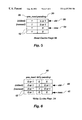
- FIG. 4 illustrates in more detail the structure of the cache portion 10 of the frame buffer memory 112 to include eight slots 12 in the SRAM, Each slot 12 can hold one block 14 of data, wherein each block 14 is comprised of four rows 16 of eight pixels 18 each.
- the cache 10 as already described, is divided into two portions, one functioning as a separate read cache 22 , and the other functioning as a separate write cache 24 .
- Implementation of read and write caches 22 , 24 as separate units provides significant advantages, as has been explained and will be further explained later.
- the presently preferred embodiment separates a read path from a write path to enable more selective manipulation of data, which reduces bus traffic.
- some cache operations do not change. For example, each read operation or any read-modify-write operation requires that data be read from the DRAM into one of the slots 12 of the SRAM 10 . If the SRAM contents have been changed (written to), that block must be written back to the DRAM before the SRAM memory space can be reused. Therefore, the cache function exists because SRAM accesses are faster than DRAM accesses. Generally, performance of such a caching system is not impacted because DRAM accesses are performed in parallel with the SRAM accesses to previous pixels.
- Separating the cache into a read portion and a write portion enables reading into cache only those blocks that are required to be read. Likewise, it also enables writing into DRAM from cache only those blocks that must be written. This feature is implemented through cache tags or flags briefly mentioned earlier.
- FIG. 5 is provided to illustrate the advantages of the separate read cache 22 . If an access to a particular slot 12 of SRAM is in the SRAM FIFO pipeline 316 (FIG. 3 ), but not yet completed, a “pending” flag 30 is set for that slot. If the slot 12 was read from the DRAM, then a “pre-read” flag 32 is set for that slot 12 . If, however, a slot 12 is used for writing only, the “pre-read” flag will be clear. A “new” pointer 34 is shown as pointing to the next available space memory. An “old” pointer 36 is shown as pointing to the next slot to free up. The cache controller 208 determines whether the data stored in the cache slot is read only. When the data is read only, it never has to be written back to the DRAM. This can save a substantial amount of time, and reduce bus traffic accordingly.
- FIG. 6 shows that the write cache 24 is implemented slightly differently because of the nature of the data. If a slot 12 of the write cache 24 has been changed, and needs to be written to the DRAM, a “dirty” flag is set for that slot until the data is written back to the DRAM. As in the case of the read cache 22 , each cache will have a “new” pointer 42 pointing to the next available slot, and an “old” pointer 44 pointed to the next slot to free up.
- Pre-reads occur, for example, when some memory accesses need a copy of a block of data stored in the DRAM. These pixel pre-read conditions exist if (1) the access is a read, (2) the access is a read-modify-write operation (such as for blending writes), or (3) a mask is being used to write only parts of a pixel.
- the cache controller 208 will set the pixel pre-read flag. This requires the use of a pre-read SRAM slot. If the block is used for a write operation only, such as a BLT destination, then the first access will be a “state full” initial write operation, which will clear all the dirty tags.
- a write operation such as a BLT destination
- the first access will be a “state full” initial write operation, which will clear all the dirty tags.
- the block is written back to DRAM, only the pixels that have been written into SRAM will be written back to the DRAM.
- pre-read collision Another condition that must be accounted for is the pre-read collision. This situation arises if, for example, a pre-read pixel needs a block that already exists as a dirty, non-pre-read block. The required pre-read function cannot occur until the dirty block is written back to DRAM. However, it is now understood that the dirty block will be written back to DRAM only after waiting for the cache pipeline to flush.
- the read and write caches when the frame buffer is needed, the read and write caches must both be checked for a match, or “hit”. If there is an address match on any of the pending slots of the write cache, a hit condition exists, and no DRAM access is required. The data will be read from the slot. On the other hand, if the access is a “read”, and there is not a match in the write cache, then the read cache is checked for an address match on a pending slot. If an address match is found, a hit condition exists again, and no DRAM access is needed.
- the no-hit condition occurs when neither the read nor the write cache have a matching pixel address.
- access to DRAM begins with a DRAM request.
- the DRAM request is written into the DRAM FIFO 320
- a pixel data access is written into the SRAM FIFO 316 (FIG. 3 ).
- the present invention can process in parallel. In other words, previous pixels in the SRAM FIFO 316 are serviced while the DRAM accesses in the DRAM FIFO 320 are being completed for the current pixels.
- the parallel processing hides the DRAM accesses from the flow of pixel data accesses.
- Efficient reuse of blocks is another important function of the present invention.
- a BLT it is common to read from a first block, write to a different block, and then read from the first block again. It is advantageous to recognize at this point that the data in the SRAM is still valid. Accordingly, it is not necessary to access DRAM again if this condition is recognizable.
- the access is a read, and no hit has been detected in either the read or write cache, the next step is to determine if the last slot that was made available on the read side is a hit, and the pre-read flag is set.
- the pre-read flag is always set on the read side except as an initial condition after reset. If there is a hit, an “old” counter is decremented by the hit logic 304 (FIG. 3 ), and that slot is reused.
- the access being a pre-read write
- the interlock logic 324 (FIG. 3) was briefly mentioned earlier and now will be discussed in more detail. As mentioned earlier, the interlock logic 324 controls synchronization of SRAM FIFO 316 and DRAM FIFO 320 . In this connection, if a pixel is a miss in the cache, it is dropped into the SRAM FIFO 316 with its sync flag set. This indicates that it was a cache miss, and must not be executed until the proper slot is loaded. At the same time that the pixel is dropped into the SRAM FIFO, the cache controller 208 loads the required block into the proper cache slot via the DRAM controller.
- the cache state machine 312 issues commands to the DRAM FIFO 320 when the functions of “access page” and “read block,” are to be performed. Specifically, “access page” is performed when there is a block-miss/page hit condition, and “read block” is performed when there is a block-miss/page-miss condition.
- the final DRAM command that is required to load the slot in the SRAM FIFO is also accompanied by a sync flag indicating that on completion of this DRAM command, the SRAM FIFO command with the corresponding sync flag may be executed.
- a set of DRAM commands is written into the DRAM FIFO with a sync flag “set” accompanying the last of such commands, and the SRAM access command that must wait for the completion of these DRAM commands is written into the SRAM FIFO with a sync flag “set” accompanying the access command.
- SRAM FIFO reads are halted if an SRAM sync flag is at the output of the SRAM FIFO before its corresponding DRAM command with sync flag set is completed.
- a sync counter (in the interlock unit 324 ) counts how many DRAM commands with sync set are completed before their corresponding SRAM access command (with sync flag set) is ready. The sync counter is decremented when the SRAM access command with sync flag set is read from the SRAM FIFO. This sync counter allows commands in the DRAM FIFO to continue irrespective of the condition of the SRAM FIFO.
- the steps of (1) executing the commands stored in the SRAM FIFO 316 , and then ( 2 ) reading data from the next SRAM FIFO location are only performed when any of the following conditions is met.
- the first condition is when the SRAM sync flag is not set, i.e., there is a hit.
- the second condition is when the sync counter is greater than 0. This means that the DRAM commands have already been executed. Accordingly, the sync counter is decremented.
- the third condition is when the DRAM sync flag is set, and the last of the corresponding DRAM commands has finished executing. In this case, the sync counter is left at 0.
Abstract
Description
Claims (11)
Priority Applications (1)
| Application Number | Priority Date | Filing Date | Title |
|---|---|---|---|
| US09/253,474 US6437789B1 (en) | 1999-02-19 | 1999-02-19 | Multi-level cache controller |
Applications Claiming Priority (1)
| Application Number | Priority Date | Filing Date | Title |
|---|---|---|---|
| US09/253,474 US6437789B1 (en) | 1999-02-19 | 1999-02-19 | Multi-level cache controller |
Publications (1)
| Publication Number | Publication Date |
|---|---|
| US6437789B1 true US6437789B1 (en) | 2002-08-20 |
Family
ID=22960424
Family Applications (1)
| Application Number | Title | Priority Date | Filing Date |
|---|---|---|---|
| US09/253,474 Expired - Fee Related US6437789B1 (en) | 1999-02-19 | 1999-02-19 | Multi-level cache controller |
Country Status (1)
| Country | Link |
|---|---|
| US (1) | US6437789B1 (en) |
Cited By (74)
| Publication number | Priority date | Publication date | Assignee | Title |
|---|---|---|---|---|
| US20020171655A1 (en) * | 2001-05-18 | 2002-11-21 | Sun Microsystems, Inc. | Dirty tag bits for 3D-RAM SRAM |
| US20030046325A1 (en) * | 2001-08-31 | 2003-03-06 | Autodesk Canada Inc. | Caching data |
| US20030129567A1 (en) * | 2001-11-29 | 2003-07-10 | Lsa, Inc. | Periscopic optical in-situ training system and method for using the same |
| US20030142101A1 (en) * | 2002-01-31 | 2003-07-31 | Lavelle Michael G. | Parallel read with source-clear operation |
| US20030160796A1 (en) * | 2002-02-28 | 2003-08-28 | Lavelle Michael G. | Active block write-back from SRAM cache to DRAM |
| US6636223B1 (en) * | 2000-08-02 | 2003-10-21 | Ati International. Srl | Graphics processing system with logic enhanced memory and method therefore |
| US6734867B1 (en) * | 2000-06-28 | 2004-05-11 | Micron Technology, Inc. | Cache invalidation method and apparatus for a graphics processing system |
| US6778179B2 (en) * | 2001-05-18 | 2004-08-17 | Sun Microsystems, Inc. | External dirty tag bits for 3D-RAM SRAM |
| US6806883B2 (en) | 2002-03-11 | 2004-10-19 | Sun Microsystems, Inc. | System and method for handling display device requests for display data from a frame buffer |
| US6812929B2 (en) | 2002-03-11 | 2004-11-02 | Sun Microsystems, Inc. | System and method for prefetching data from a frame buffer |
| US20050169291A1 (en) * | 2002-04-30 | 2005-08-04 | Key Kenneth M. | System and method for operating a packet buffer in an intermediate node |
| US20050231519A1 (en) * | 1999-03-22 | 2005-10-20 | Gopal Solanki | Texture caching arrangement for a computer graphics accelerator |
| US20050240745A1 (en) * | 2003-12-18 | 2005-10-27 | Sundar Iyer | High speed memory control and I/O processor system |
| US20050280652A1 (en) * | 2004-05-14 | 2005-12-22 | Hutchins Edward A | System and method for a universal data write unit in a 3-D graphics pipeline including generic cache memories |
| US20060031565A1 (en) * | 2004-07-16 | 2006-02-09 | Sundar Iyer | High speed packet-buffering system |
| US20060103659A1 (en) * | 2004-11-15 | 2006-05-18 | Ashish Karandikar | Latency tolerant system for executing video processing operations |
| US7050060B1 (en) * | 1999-10-07 | 2006-05-23 | International Business Machines Corporation | Data transferring apparatus and its method |
| US20060250408A1 (en) * | 2005-05-06 | 2006-11-09 | Via Technologies, Inc. | Texture cache control using an adaptive missing data table in a multiple cache computer graphics environment |
| US20070153014A1 (en) * | 2005-12-30 | 2007-07-05 | Sabol Mark A | Method and system for symmetric allocation for a shared L2 mapping cache |
| US20080147980A1 (en) * | 2005-02-15 | 2008-06-19 | Koninklijke Philips Electronics, N.V. | Enhancing Performance of a Memory Unit of a Data Processing Device By Separating Reading and Fetching Functionalities |
| US20080298372A1 (en) * | 2004-02-05 | 2008-12-04 | International Business Machines Corporation | Structure and method for scheduler pipeline design for hierarchical link sharing |
| US20100153661A1 (en) * | 2008-12-11 | 2010-06-17 | Nvidia Corporation | Processing of read requests in a memory controller using pre-fetch mechanism |
| US7868902B1 (en) | 2004-05-14 | 2011-01-11 | Nvidia Corporation | System and method for pixel data row forwarding in a 3-D graphics pipeline |
| US7891818B2 (en) | 2006-12-12 | 2011-02-22 | Evans & Sutherland Computer Corporation | System and method for aligning RGB light in a single modulator projector |
| US8077378B1 (en) | 2008-11-12 | 2011-12-13 | Evans & Sutherland Computer Corporation | Calibration system and method for light modulation device |
| US8358317B2 (en) | 2008-05-23 | 2013-01-22 | Evans & Sutherland Computer Corporation | System and method for displaying a planar image on a curved surface |
| US8411096B1 (en) | 2007-08-15 | 2013-04-02 | Nvidia Corporation | Shader program instruction fetch |
| US8427490B1 (en) | 2004-05-14 | 2013-04-23 | Nvidia Corporation | Validating a graphics pipeline using pre-determined schedules |
| US20130318291A1 (en) * | 2012-05-22 | 2013-11-28 | Gerald Pepper | Methods, systems, and computer readable media for generating test packets in a network test device using value list caching |
| US8624906B2 (en) | 2004-09-29 | 2014-01-07 | Nvidia Corporation | Method and system for non stalling pipeline instruction fetching from memory |
| US20140032846A1 (en) * | 2012-07-30 | 2014-01-30 | Soft Machines, Inc. | Systems and methods for supporting a plurality of load and store accesses of a cache |
| US8659601B1 (en) | 2007-08-15 | 2014-02-25 | Nvidia Corporation | Program sequencer for generating indeterminant length shader programs for a graphics processor |
| US8681861B2 (en) | 2008-05-01 | 2014-03-25 | Nvidia Corporation | Multistandard hardware video encoder |
| US8683126B2 (en) | 2007-07-30 | 2014-03-25 | Nvidia Corporation | Optimal use of buffer space by a storage controller which writes retrieved data directly to a memory |
| US8698819B1 (en) | 2007-08-15 | 2014-04-15 | Nvidia Corporation | Software assisted shader merging |
| US8702248B1 (en) | 2008-06-11 | 2014-04-22 | Evans & Sutherland Computer Corporation | Projection method for reducing interpixel gaps on a viewing surface |
| US8780123B2 (en) | 2007-12-17 | 2014-07-15 | Nvidia Corporation | Interrupt handling techniques in the rasterizer of a GPU |
| US8923385B2 (en) | 2008-05-01 | 2014-12-30 | Nvidia Corporation | Rewind-enabled hardware encoder |
| US8930674B2 (en) | 2012-03-07 | 2015-01-06 | Soft Machines, Inc. | Systems and methods for accessing a unified translation lookaside buffer |
| US9024957B1 (en) | 2007-08-15 | 2015-05-05 | Nvidia Corporation | Address independent shader program loading |
| US9064333B2 (en) | 2007-12-17 | 2015-06-23 | Nvidia Corporation | Interrupt handling techniques in the rasterizer of a GPU |
| US9092170B1 (en) | 2005-10-18 | 2015-07-28 | Nvidia Corporation | Method and system for implementing fragment operation processing across a graphics bus interconnect |
| US20150332078A1 (en) * | 2009-10-01 | 2015-11-19 | Hand Held Products, Inc. | Low power multi-core decoder system and method |
| US20150370706A1 (en) * | 2014-06-18 | 2015-12-24 | International Business Machines Corporation | Method and apparatus for cache memory data processing |
| US9430410B2 (en) | 2012-07-30 | 2016-08-30 | Soft Machines, Inc. | Systems and methods for supporting a plurality of load accesses of a cache in a single cycle |
| US20170115930A1 (en) * | 2015-10-22 | 2017-04-27 | International Business Machines Corporation | Distributed serialized data buffer and a memory module for a cascadable and extended memory subsystem |
| US9641826B1 (en) | 2011-10-06 | 2017-05-02 | Evans & Sutherland Computer Corporation | System and method for displaying distant 3-D stereo on a dome surface |
| US9678882B2 (en) | 2012-10-11 | 2017-06-13 | Intel Corporation | Systems and methods for non-blocking implementation of cache flush instructions |
| US9710399B2 (en) | 2012-07-30 | 2017-07-18 | Intel Corporation | Systems and methods for flushing a cache with modified data |
| US9720831B2 (en) | 2012-07-30 | 2017-08-01 | Intel Corporation | Systems and methods for maintaining the coherency of a store coalescing cache and a load cache |
| US9766893B2 (en) | 2011-03-25 | 2017-09-19 | Intel Corporation | Executing instruction sequence code blocks by using virtual cores instantiated by partitionable engines |
| US9811342B2 (en) | 2013-03-15 | 2017-11-07 | Intel Corporation | Method for performing dual dispatch of blocks and half blocks |
| US9811377B2 (en) | 2013-03-15 | 2017-11-07 | Intel Corporation | Method for executing multithreaded instructions grouped into blocks |
| US9823930B2 (en) | 2013-03-15 | 2017-11-21 | Intel Corporation | Method for emulating a guest centralized flag architecture by using a native distributed flag architecture |
| US9842005B2 (en) | 2011-03-25 | 2017-12-12 | Intel Corporation | Register file segments for supporting code block execution by using virtual cores instantiated by partitionable engines |
| US9858080B2 (en) | 2013-03-15 | 2018-01-02 | Intel Corporation | Method for implementing a reduced size register view data structure in a microprocessor |
| US9886416B2 (en) | 2006-04-12 | 2018-02-06 | Intel Corporation | Apparatus and method for processing an instruction matrix specifying parallel and dependent operations |
| US9886279B2 (en) | 2013-03-15 | 2018-02-06 | Intel Corporation | Method for populating and instruction view data structure by using register template snapshots |
| US9891924B2 (en) | 2013-03-15 | 2018-02-13 | Intel Corporation | Method for implementing a reduced size register view data structure in a microprocessor |
| US9898412B2 (en) | 2013-03-15 | 2018-02-20 | Intel Corporation | Methods, systems and apparatus for predicting the way of a set associative cache |
| US9916253B2 (en) | 2012-07-30 | 2018-03-13 | Intel Corporation | Method and apparatus for supporting a plurality of load accesses of a cache in a single cycle to maintain throughput |
| US9921845B2 (en) | 2011-03-25 | 2018-03-20 | Intel Corporation | Memory fragments for supporting code block execution by using virtual cores instantiated by partitionable engines |
| US9934042B2 (en) | 2013-03-15 | 2018-04-03 | Intel Corporation | Method for dependency broadcasting through a block organized source view data structure |
| US9940134B2 (en) | 2011-05-20 | 2018-04-10 | Intel Corporation | Decentralized allocation of resources and interconnect structures to support the execution of instruction sequences by a plurality of engines |
| US9965281B2 (en) | 2006-11-14 | 2018-05-08 | Intel Corporation | Cache storing data fetched by address calculating load instruction with label used as associated name for consuming instruction to refer |
| US10031784B2 (en) | 2011-05-20 | 2018-07-24 | Intel Corporation | Interconnect system to support the execution of instruction sequences by a plurality of partitionable engines |
| US10140138B2 (en) | 2013-03-15 | 2018-11-27 | Intel Corporation | Methods, systems and apparatus for supporting wide and efficient front-end operation with guest-architecture emulation |
| US10146548B2 (en) | 2013-03-15 | 2018-12-04 | Intel Corporation | Method for populating a source view data structure by using register template snapshots |
| US10169045B2 (en) | 2013-03-15 | 2019-01-01 | Intel Corporation | Method for dependency broadcasting through a source organized source view data structure |
| US10191746B2 (en) | 2011-11-22 | 2019-01-29 | Intel Corporation | Accelerated code optimizer for a multiengine microprocessor |
| US10198266B2 (en) | 2013-03-15 | 2019-02-05 | Intel Corporation | Method for populating register view data structure by using register template snapshots |
| US10229043B2 (en) | 2013-07-23 | 2019-03-12 | Intel Business Machines Corporation | Requesting memory spaces and resources using a memory controller |
| US10228949B2 (en) | 2010-09-17 | 2019-03-12 | Intel Corporation | Single cycle multi-branch prediction including shadow cache for early far branch prediction |
| US10521239B2 (en) | 2011-11-22 | 2019-12-31 | Intel Corporation | Microprocessor accelerated code optimizer |
Citations (13)
| Publication number | Priority date | Publication date | Assignee | Title |
|---|---|---|---|---|
| US5276849A (en) * | 1989-09-11 | 1994-01-04 | Wang Laboratories, Inc. | Apparatus and method for maintaining cache/main memory consistency utilizing a dual port FIFO buffer |
| US5430888A (en) | 1988-07-25 | 1995-07-04 | Digital Equipment Corporation | Pipeline utilizing an integral cache for transferring data to and from a register |
| US5544306A (en) * | 1994-05-03 | 1996-08-06 | Sun Microsystems, Inc. | Flexible dram access in a frame buffer memory and system |
| US5544340A (en) | 1990-06-01 | 1996-08-06 | Hitachi, Ltd. | Method and system for controlling cache memory with a storage buffer to increase throughput of a write operation to the cache memory |
| US5557733A (en) * | 1993-04-02 | 1996-09-17 | Vlsi Technology, Inc. | Caching FIFO and method therefor |
| US5559952A (en) * | 1993-03-23 | 1996-09-24 | Kabushiki Kaisha Toshiba | Display controller incorporating cache memory dedicated for VRAM |
| US5586291A (en) * | 1994-12-23 | 1996-12-17 | Emc Corporation | Disk controller with volatile and non-volatile cache memories |
| US5598517A (en) | 1995-01-10 | 1997-01-28 | Evans & Sutherland Computer Corp. | Computer graphics pixel rendering system with multi-level scanning |
| US5696947A (en) * | 1995-11-20 | 1997-12-09 | International Business Machines Corporation | Two dimensional frame buffer memory interface system and method of operation thereof |
| US5734386A (en) | 1995-09-08 | 1998-03-31 | Evans & Sutherland Computer Corporation | System and method for displaying textured polygons using planar texture interpolation |
| US5761709A (en) * | 1995-06-05 | 1998-06-02 | Advanced Micro Devices, Inc. | Write cache for servicing write requests within a predetermined address range |
| US5909225A (en) * | 1997-05-30 | 1999-06-01 | Hewlett-Packard Co. | Frame buffer cache for graphics applications |
| US6141025A (en) * | 1996-02-06 | 2000-10-31 | Sony Computer Entertainment, Inc. | Image generating apparatus with FIFO memory and cache memory |
-
1999
- 1999-02-19 US US09/253,474 patent/US6437789B1/en not_active Expired - Fee Related
Patent Citations (13)
| Publication number | Priority date | Publication date | Assignee | Title |
|---|---|---|---|---|
| US5430888A (en) | 1988-07-25 | 1995-07-04 | Digital Equipment Corporation | Pipeline utilizing an integral cache for transferring data to and from a register |
| US5276849A (en) * | 1989-09-11 | 1994-01-04 | Wang Laboratories, Inc. | Apparatus and method for maintaining cache/main memory consistency utilizing a dual port FIFO buffer |
| US5544340A (en) | 1990-06-01 | 1996-08-06 | Hitachi, Ltd. | Method and system for controlling cache memory with a storage buffer to increase throughput of a write operation to the cache memory |
| US5559952A (en) * | 1993-03-23 | 1996-09-24 | Kabushiki Kaisha Toshiba | Display controller incorporating cache memory dedicated for VRAM |
| US5557733A (en) * | 1993-04-02 | 1996-09-17 | Vlsi Technology, Inc. | Caching FIFO and method therefor |
| US5544306A (en) * | 1994-05-03 | 1996-08-06 | Sun Microsystems, Inc. | Flexible dram access in a frame buffer memory and system |
| US5586291A (en) * | 1994-12-23 | 1996-12-17 | Emc Corporation | Disk controller with volatile and non-volatile cache memories |
| US5598517A (en) | 1995-01-10 | 1997-01-28 | Evans & Sutherland Computer Corp. | Computer graphics pixel rendering system with multi-level scanning |
| US5761709A (en) * | 1995-06-05 | 1998-06-02 | Advanced Micro Devices, Inc. | Write cache for servicing write requests within a predetermined address range |
| US5734386A (en) | 1995-09-08 | 1998-03-31 | Evans & Sutherland Computer Corporation | System and method for displaying textured polygons using planar texture interpolation |
| US5696947A (en) * | 1995-11-20 | 1997-12-09 | International Business Machines Corporation | Two dimensional frame buffer memory interface system and method of operation thereof |
| US6141025A (en) * | 1996-02-06 | 2000-10-31 | Sony Computer Entertainment, Inc. | Image generating apparatus with FIFO memory and cache memory |
| US5909225A (en) * | 1997-05-30 | 1999-06-01 | Hewlett-Packard Co. | Frame buffer cache for graphics applications |
Non-Patent Citations (2)
| Title |
|---|
| Deering et al., "FBRAM: A new Form of Memory Optimized for 3D Graphics", Computer Graphics Proceedings, Annual Conference Series, 1994. |
| Mitsubishi Electronics Device Group, 3D-RAM, "Overview of 3D-RAM and Its Funcitonal Blocks". |
Cited By (145)
| Publication number | Priority date | Publication date | Assignee | Title |
|---|---|---|---|---|
| US8018467B2 (en) | 1999-03-22 | 2011-09-13 | Nvidia Corporation | Texture caching arrangement for a computer graphics accelerator |
| US20050231519A1 (en) * | 1999-03-22 | 2005-10-20 | Gopal Solanki | Texture caching arrangement for a computer graphics accelerator |
| US7330188B1 (en) * | 1999-03-22 | 2008-02-12 | Nvidia Corp | Texture caching arrangement for a computer graphics accelerator |
| US7050060B1 (en) * | 1999-10-07 | 2006-05-23 | International Business Machines Corporation | Data transferring apparatus and its method |
| US6734867B1 (en) * | 2000-06-28 | 2004-05-11 | Micron Technology, Inc. | Cache invalidation method and apparatus for a graphics processing system |
| US6937246B2 (en) | 2000-06-28 | 2005-08-30 | Micron Technology, Inc. | Cache invalidation method and apparatus for a graphics processing system |
| US20040155885A1 (en) * | 2000-06-28 | 2004-08-12 | Aaftab Munshi | Cache invalidation method and apparatus for a graphics processing system |
| US6636223B1 (en) * | 2000-08-02 | 2003-10-21 | Ati International. Srl | Graphics processing system with logic enhanced memory and method therefore |
| US6778179B2 (en) * | 2001-05-18 | 2004-08-17 | Sun Microsystems, Inc. | External dirty tag bits for 3D-RAM SRAM |
| US20020171655A1 (en) * | 2001-05-18 | 2002-11-21 | Sun Microsystems, Inc. | Dirty tag bits for 3D-RAM SRAM |
| US6720969B2 (en) * | 2001-05-18 | 2004-04-13 | Sun Microsystems, Inc. | Dirty tag bits for 3D-RAM SRAM |
| US20030046325A1 (en) * | 2001-08-31 | 2003-03-06 | Autodesk Canada Inc. | Caching data |
| US6910103B2 (en) * | 2001-08-31 | 2005-06-21 | Autodesk Canada Inc. | Caching data |
| US7056119B2 (en) | 2001-11-29 | 2006-06-06 | Lsa, Inc. | Periscopic optical training system for operators of vehicles |
| US20030129567A1 (en) * | 2001-11-29 | 2003-07-10 | Lsa, Inc. | Periscopic optical in-situ training system and method for using the same |
| US6795078B2 (en) * | 2002-01-31 | 2004-09-21 | Sun Microsystems, Inc. | Parallel read with source-clear operation |
| US20030142101A1 (en) * | 2002-01-31 | 2003-07-31 | Lavelle Michael G. | Parallel read with source-clear operation |
| US20030160796A1 (en) * | 2002-02-28 | 2003-08-28 | Lavelle Michael G. | Active block write-back from SRAM cache to DRAM |
| US7027064B2 (en) * | 2002-02-28 | 2006-04-11 | Sun Microsystems, Inc. | Active block write-back from SRAM cache to DRAM |
| US6812929B2 (en) | 2002-03-11 | 2004-11-02 | Sun Microsystems, Inc. | System and method for prefetching data from a frame buffer |
| US6806883B2 (en) | 2002-03-11 | 2004-10-19 | Sun Microsystems, Inc. | System and method for handling display device requests for display data from a frame buffer |
| US20050169291A1 (en) * | 2002-04-30 | 2005-08-04 | Key Kenneth M. | System and method for operating a packet buffer in an intermediate node |
| US8180966B2 (en) * | 2002-04-30 | 2012-05-15 | Cisco Technology, Inc. | System and method for operating a packet buffer in an intermediate node |
| USRE45097E1 (en) | 2003-12-18 | 2014-08-26 | Cisco Technology, Inc. | High speed memory and input/output processor subsystem for efficiently allocating and using high-speed memory and slower-speed memory |
| US20050240745A1 (en) * | 2003-12-18 | 2005-10-27 | Sundar Iyer | High speed memory control and I/O processor system |
| US7657706B2 (en) * | 2003-12-18 | 2010-02-02 | Cisco Technology, Inc. | High speed memory and input/output processor subsystem for efficiently allocating and using high-speed memory and slower-speed memory |
| US7929438B2 (en) * | 2004-02-05 | 2011-04-19 | International Business Machines Corporation | Scheduler pipeline design for hierarchical link sharing |
| US20080298372A1 (en) * | 2004-02-05 | 2008-12-04 | International Business Machines Corporation | Structure and method for scheduler pipeline design for hierarchical link sharing |
| EP1756803A4 (en) * | 2004-05-14 | 2009-01-07 | Nvidia Corp | System and method for a universal data write unit |
| US7724263B2 (en) | 2004-05-14 | 2010-05-25 | Nvidia Corporation | System and method for a universal data write unit in a 3-D graphics pipeline including generic cache memories |
| US8427490B1 (en) | 2004-05-14 | 2013-04-23 | Nvidia Corporation | Validating a graphics pipeline using pre-determined schedules |
| EP1756803A2 (en) * | 2004-05-14 | 2007-02-28 | Nvidia Corporation | System and method for a universal data write unit |
| US20050280652A1 (en) * | 2004-05-14 | 2005-12-22 | Hutchins Edward A | System and method for a universal data write unit in a 3-D graphics pipeline including generic cache memories |
| US7868902B1 (en) | 2004-05-14 | 2011-01-11 | Nvidia Corporation | System and method for pixel data row forwarding in a 3-D graphics pipeline |
| US20060031565A1 (en) * | 2004-07-16 | 2006-02-09 | Sundar Iyer | High speed packet-buffering system |
| US8624906B2 (en) | 2004-09-29 | 2014-01-07 | Nvidia Corporation | Method and system for non stalling pipeline instruction fetching from memory |
| US8736623B1 (en) | 2004-11-15 | 2014-05-27 | Nvidia Corporation | Programmable DMA engine for implementing memory transfers and video processing for a video processor |
| US8687008B2 (en) | 2004-11-15 | 2014-04-01 | Nvidia Corporation | Latency tolerant system for executing video processing operations |
| US8698817B2 (en) | 2004-11-15 | 2014-04-15 | Nvidia Corporation | Video processor having scalar and vector components |
| US8725990B1 (en) | 2004-11-15 | 2014-05-13 | Nvidia Corporation | Configurable SIMD engine with high, low and mixed precision modes |
| US20060176308A1 (en) * | 2004-11-15 | 2006-08-10 | Ashish Karandikar | Multidimensional datapath processing in a video processor |
| US20060176309A1 (en) * | 2004-11-15 | 2006-08-10 | Shirish Gadre | Video processor having scalar and vector components |
| US8683184B1 (en) | 2004-11-15 | 2014-03-25 | Nvidia Corporation | Multi context execution on a video processor |
| US20060103659A1 (en) * | 2004-11-15 | 2006-05-18 | Ashish Karandikar | Latency tolerant system for executing video processing operations |
| US8416251B2 (en) | 2004-11-15 | 2013-04-09 | Nvidia Corporation | Stream processing in a video processor |
| US9111368B1 (en) | 2004-11-15 | 2015-08-18 | Nvidia Corporation | Pipelined L2 cache for memory transfers for a video processor |
| US8493396B2 (en) | 2004-11-15 | 2013-07-23 | Nvidia Corporation | Multidimensional datapath processing in a video processor |
| US8424012B1 (en) | 2004-11-15 | 2013-04-16 | Nvidia Corporation | Context switching on a video processor having a scalar execution unit and a vector execution unit |
| US8738891B1 (en) | 2004-11-15 | 2014-05-27 | Nvidia Corporation | Methods and systems for command acceleration in a video processor via translation of scalar instructions into vector instructions |
| US8493397B1 (en) * | 2004-11-15 | 2013-07-23 | Nvidia Corporation | State machine control for a pipelined L2 cache to implement memory transfers for a video processor |
| US7797493B2 (en) | 2005-02-15 | 2010-09-14 | Koninklijke Philips Electronics N.V. | Enhancing performance of a memory unit of a data processing device by separating reading and fetching functionalities |
| US20080147980A1 (en) * | 2005-02-15 | 2008-06-19 | Koninklijke Philips Electronics, N.V. | Enhancing Performance of a Memory Unit of a Data Processing Device By Separating Reading and Fetching Functionalities |
| US7348988B2 (en) * | 2005-05-06 | 2008-03-25 | Via Technologies, Inc. | Texture cache control using an adaptive missing data table in a multiple cache computer graphics environment |
| US20060250408A1 (en) * | 2005-05-06 | 2006-11-09 | Via Technologies, Inc. | Texture cache control using an adaptive missing data table in a multiple cache computer graphics environment |
| US9092170B1 (en) | 2005-10-18 | 2015-07-28 | Nvidia Corporation | Method and system for implementing fragment operation processing across a graphics bus interconnect |
| US20070153014A1 (en) * | 2005-12-30 | 2007-07-05 | Sabol Mark A | Method and system for symmetric allocation for a shared L2 mapping cache |
| US8593474B2 (en) * | 2005-12-30 | 2013-11-26 | Intel Corporation | Method and system for symmetric allocation for a shared L2 mapping cache |
| US11163720B2 (en) | 2006-04-12 | 2021-11-02 | Intel Corporation | Apparatus and method for processing an instruction matrix specifying parallel and dependent operations |
| US9886416B2 (en) | 2006-04-12 | 2018-02-06 | Intel Corporation | Apparatus and method for processing an instruction matrix specifying parallel and dependent operations |
| US10289605B2 (en) | 2006-04-12 | 2019-05-14 | Intel Corporation | Apparatus and method for processing an instruction matrix specifying parallel and dependent operations |
| US10585670B2 (en) | 2006-11-14 | 2020-03-10 | Intel Corporation | Cache storing data fetched by address calculating load instruction with label used as associated name for consuming instruction to refer |
| US9965281B2 (en) | 2006-11-14 | 2018-05-08 | Intel Corporation | Cache storing data fetched by address calculating load instruction with label used as associated name for consuming instruction to refer |
| US7891818B2 (en) | 2006-12-12 | 2011-02-22 | Evans & Sutherland Computer Corporation | System and method for aligning RGB light in a single modulator projector |
| US8683126B2 (en) | 2007-07-30 | 2014-03-25 | Nvidia Corporation | Optimal use of buffer space by a storage controller which writes retrieved data directly to a memory |
| US9024957B1 (en) | 2007-08-15 | 2015-05-05 | Nvidia Corporation | Address independent shader program loading |
| US8698819B1 (en) | 2007-08-15 | 2014-04-15 | Nvidia Corporation | Software assisted shader merging |
| US8411096B1 (en) | 2007-08-15 | 2013-04-02 | Nvidia Corporation | Shader program instruction fetch |
| US8659601B1 (en) | 2007-08-15 | 2014-02-25 | Nvidia Corporation | Program sequencer for generating indeterminant length shader programs for a graphics processor |
| US8780123B2 (en) | 2007-12-17 | 2014-07-15 | Nvidia Corporation | Interrupt handling techniques in the rasterizer of a GPU |
| US9064333B2 (en) | 2007-12-17 | 2015-06-23 | Nvidia Corporation | Interrupt handling techniques in the rasterizer of a GPU |
| US8681861B2 (en) | 2008-05-01 | 2014-03-25 | Nvidia Corporation | Multistandard hardware video encoder |
| US8923385B2 (en) | 2008-05-01 | 2014-12-30 | Nvidia Corporation | Rewind-enabled hardware encoder |
| US8358317B2 (en) | 2008-05-23 | 2013-01-22 | Evans & Sutherland Computer Corporation | System and method for displaying a planar image on a curved surface |
| US8702248B1 (en) | 2008-06-11 | 2014-04-22 | Evans & Sutherland Computer Corporation | Projection method for reducing interpixel gaps on a viewing surface |
| US8077378B1 (en) | 2008-11-12 | 2011-12-13 | Evans & Sutherland Computer Corporation | Calibration system and method for light modulation device |
| US8489851B2 (en) | 2008-12-11 | 2013-07-16 | Nvidia Corporation | Processing of read requests in a memory controller using pre-fetch mechanism |
| US20100153661A1 (en) * | 2008-12-11 | 2010-06-17 | Nvidia Corporation | Processing of read requests in a memory controller using pre-fetch mechanism |
| US20150332078A1 (en) * | 2009-10-01 | 2015-11-19 | Hand Held Products, Inc. | Low power multi-core decoder system and method |
| US9384378B2 (en) * | 2009-10-01 | 2016-07-05 | Hand Held Products, Inc. | Low power multi-core decoder system and method |
| US9659203B2 (en) | 2009-10-01 | 2017-05-23 | Hand Held Products, Inc. | Low power multi-core decoder system and method |
| US10228949B2 (en) | 2010-09-17 | 2019-03-12 | Intel Corporation | Single cycle multi-branch prediction including shadow cache for early far branch prediction |
| US10564975B2 (en) | 2011-03-25 | 2020-02-18 | Intel Corporation | Memory fragments for supporting code block execution by using virtual cores instantiated by partitionable engines |
| US9934072B2 (en) | 2011-03-25 | 2018-04-03 | Intel Corporation | Register file segments for supporting code block execution by using virtual cores instantiated by partitionable engines |
| US11204769B2 (en) | 2011-03-25 | 2021-12-21 | Intel Corporation | Memory fragments for supporting code block execution by using virtual cores instantiated by partitionable engines |
| US9842005B2 (en) | 2011-03-25 | 2017-12-12 | Intel Corporation | Register file segments for supporting code block execution by using virtual cores instantiated by partitionable engines |
| US9990200B2 (en) | 2011-03-25 | 2018-06-05 | Intel Corporation | Executing instruction sequence code blocks by using virtual cores instantiated by partitionable engines |
| US9766893B2 (en) | 2011-03-25 | 2017-09-19 | Intel Corporation | Executing instruction sequence code blocks by using virtual cores instantiated by partitionable engines |
| US9921845B2 (en) | 2011-03-25 | 2018-03-20 | Intel Corporation | Memory fragments for supporting code block execution by using virtual cores instantiated by partitionable engines |
| US9940134B2 (en) | 2011-05-20 | 2018-04-10 | Intel Corporation | Decentralized allocation of resources and interconnect structures to support the execution of instruction sequences by a plurality of engines |
| US10031784B2 (en) | 2011-05-20 | 2018-07-24 | Intel Corporation | Interconnect system to support the execution of instruction sequences by a plurality of partitionable engines |
| US10372454B2 (en) | 2011-05-20 | 2019-08-06 | Intel Corporation | Allocation of a segmented interconnect to support the execution of instruction sequences by a plurality of engines |
| US10110876B1 (en) | 2011-10-06 | 2018-10-23 | Evans & Sutherland Computer Corporation | System and method for displaying images in 3-D stereo |
| US9641826B1 (en) | 2011-10-06 | 2017-05-02 | Evans & Sutherland Computer Corporation | System and method for displaying distant 3-D stereo on a dome surface |
| US10191746B2 (en) | 2011-11-22 | 2019-01-29 | Intel Corporation | Accelerated code optimizer for a multiengine microprocessor |
| US10521239B2 (en) | 2011-11-22 | 2019-12-31 | Intel Corporation | Microprocessor accelerated code optimizer |
| US9454491B2 (en) | 2012-03-07 | 2016-09-27 | Soft Machines Inc. | Systems and methods for accessing a unified translation lookaside buffer |
| US9767038B2 (en) | 2012-03-07 | 2017-09-19 | Intel Corporation | Systems and methods for accessing a unified translation lookaside buffer |
| US10310987B2 (en) | 2012-03-07 | 2019-06-04 | Intel Corporation | Systems and methods for accessing a unified translation lookaside buffer |
| US8930674B2 (en) | 2012-03-07 | 2015-01-06 | Soft Machines, Inc. | Systems and methods for accessing a unified translation lookaside buffer |
| US20130318291A1 (en) * | 2012-05-22 | 2013-11-28 | Gerald Pepper | Methods, systems, and computer readable media for generating test packets in a network test device using value list caching |
| US9491081B2 (en) * | 2012-05-22 | 2016-11-08 | Ixia | Methods, systems, and computer readable media for generating test packets in a network test device using value list caching |
| US10210101B2 (en) | 2012-07-30 | 2019-02-19 | Intel Corporation | Systems and methods for flushing a cache with modified data |
| US10346302B2 (en) | 2012-07-30 | 2019-07-09 | Intel Corporation | Systems and methods for maintaining the coherency of a store coalescing cache and a load cache |
| US20140032846A1 (en) * | 2012-07-30 | 2014-01-30 | Soft Machines, Inc. | Systems and methods for supporting a plurality of load and store accesses of a cache |
| US10698833B2 (en) | 2012-07-30 | 2020-06-30 | Intel Corporation | Method and apparatus for supporting a plurality of load accesses of a cache in a single cycle to maintain throughput |
| US9720831B2 (en) | 2012-07-30 | 2017-08-01 | Intel Corporation | Systems and methods for maintaining the coherency of a store coalescing cache and a load cache |
| US9229873B2 (en) * | 2012-07-30 | 2016-01-05 | Soft Machines, Inc. | Systems and methods for supporting a plurality of load and store accesses of a cache |
| US20160041913A1 (en) * | 2012-07-30 | 2016-02-11 | Soft Machines, Inc. | Systems and methods for supporting a plurality of load and store accesses of a cache |
| US9916253B2 (en) | 2012-07-30 | 2018-03-13 | Intel Corporation | Method and apparatus for supporting a plurality of load accesses of a cache in a single cycle to maintain throughput |
| US9740612B2 (en) | 2012-07-30 | 2017-08-22 | Intel Corporation | Systems and methods for maintaining the coherency of a store coalescing cache and a load cache |
| US9430410B2 (en) | 2012-07-30 | 2016-08-30 | Soft Machines, Inc. | Systems and methods for supporting a plurality of load accesses of a cache in a single cycle |
| US9720839B2 (en) * | 2012-07-30 | 2017-08-01 | Intel Corporation | Systems and methods for supporting a plurality of load and store accesses of a cache |
| US9858206B2 (en) | 2012-07-30 | 2018-01-02 | Intel Corporation | Systems and methods for flushing a cache with modified data |
| US9710399B2 (en) | 2012-07-30 | 2017-07-18 | Intel Corporation | Systems and methods for flushing a cache with modified data |
| US9678882B2 (en) | 2012-10-11 | 2017-06-13 | Intel Corporation | Systems and methods for non-blocking implementation of cache flush instructions |
| US9842056B2 (en) | 2012-10-11 | 2017-12-12 | Intel Corporation | Systems and methods for non-blocking implementation of cache flush instructions |
| US10585804B2 (en) | 2012-10-11 | 2020-03-10 | Intel Corporation | Systems and methods for non-blocking implementation of cache flush instructions |
| US9811377B2 (en) | 2013-03-15 | 2017-11-07 | Intel Corporation | Method for executing multithreaded instructions grouped into blocks |
| US9904625B2 (en) | 2013-03-15 | 2018-02-27 | Intel Corporation | Methods, systems and apparatus for predicting the way of a set associative cache |
| US10146548B2 (en) | 2013-03-15 | 2018-12-04 | Intel Corporation | Method for populating a source view data structure by using register template snapshots |
| US10146576B2 (en) | 2013-03-15 | 2018-12-04 | Intel Corporation | Method for executing multithreaded instructions grouped into blocks |
| US10169045B2 (en) | 2013-03-15 | 2019-01-01 | Intel Corporation | Method for dependency broadcasting through a source organized source view data structure |
| US11656875B2 (en) | 2013-03-15 | 2023-05-23 | Intel Corporation | Method and system for instruction block to execution unit grouping |
| US10198266B2 (en) | 2013-03-15 | 2019-02-05 | Intel Corporation | Method for populating register view data structure by using register template snapshots |
| US9858080B2 (en) | 2013-03-15 | 2018-01-02 | Intel Corporation | Method for implementing a reduced size register view data structure in a microprocessor |
| US10740126B2 (en) | 2013-03-15 | 2020-08-11 | Intel Corporation | Methods, systems and apparatus for supporting wide and efficient front-end operation with guest-architecture emulation |
| US9886279B2 (en) | 2013-03-15 | 2018-02-06 | Intel Corporation | Method for populating and instruction view data structure by using register template snapshots |
| US10248570B2 (en) | 2013-03-15 | 2019-04-02 | Intel Corporation | Methods, systems and apparatus for predicting the way of a set associative cache |
| US10255076B2 (en) | 2013-03-15 | 2019-04-09 | Intel Corporation | Method for performing dual dispatch of blocks and half blocks |
| US9891924B2 (en) | 2013-03-15 | 2018-02-13 | Intel Corporation | Method for implementing a reduced size register view data structure in a microprocessor |
| US10275255B2 (en) | 2013-03-15 | 2019-04-30 | Intel Corporation | Method for dependency broadcasting through a source organized source view data structure |
| US9811342B2 (en) | 2013-03-15 | 2017-11-07 | Intel Corporation | Method for performing dual dispatch of blocks and half blocks |
| US9898412B2 (en) | 2013-03-15 | 2018-02-20 | Intel Corporation | Methods, systems and apparatus for predicting the way of a set associative cache |
| US9934042B2 (en) | 2013-03-15 | 2018-04-03 | Intel Corporation | Method for dependency broadcasting through a block organized source view data structure |
| US9823930B2 (en) | 2013-03-15 | 2017-11-21 | Intel Corporation | Method for emulating a guest centralized flag architecture by using a native distributed flag architecture |
| US10503514B2 (en) | 2013-03-15 | 2019-12-10 | Intel Corporation | Method for implementing a reduced size register view data structure in a microprocessor |
| US10140138B2 (en) | 2013-03-15 | 2018-11-27 | Intel Corporation | Methods, systems and apparatus for supporting wide and efficient front-end operation with guest-architecture emulation |
| US10275348B2 (en) | 2013-07-23 | 2019-04-30 | International Business Machines Corporation | Memory controller for requesting memory spaces and resources |
| US10229043B2 (en) | 2013-07-23 | 2019-03-12 | Intel Business Machines Corporation | Requesting memory spaces and resources using a memory controller |
| US20150370711A1 (en) * | 2014-06-18 | 2015-12-24 | International Business Machines Corporation | Method and apparatus for cache memory data processing |
| US9792209B2 (en) * | 2014-06-18 | 2017-10-17 | International Business Machines Corporation | Method and apparatus for cache memory data processing |
| US20150370706A1 (en) * | 2014-06-18 | 2015-12-24 | International Business Machines Corporation | Method and apparatus for cache memory data processing |
| US9710381B2 (en) * | 2014-06-18 | 2017-07-18 | International Business Machines Corporation | Method and apparatus for cache memory data processing |
| US20170115930A1 (en) * | 2015-10-22 | 2017-04-27 | International Business Machines Corporation | Distributed serialized data buffer and a memory module for a cascadable and extended memory subsystem |
| US10102884B2 (en) * | 2015-10-22 | 2018-10-16 | International Business Machines Corporation | Distributed serialized data buffer and a memory module for a cascadable and extended memory subsystem |
Similar Documents
| Publication | Publication Date | Title |
|---|---|---|
| US6437789B1 (en) | Multi-level cache controller | |
| JP3828184B2 (en) | Frame buffer memory device controller | |
| US7383412B1 (en) | On-demand memory synchronization for peripheral systems with multiple parallel processors | |
| US6564304B1 (en) | Memory processing system and method for accessing memory including reordering memory requests to reduce mode switching | |
| US6591347B2 (en) | Dynamic replacement technique in a shared cache | |
| US6434639B1 (en) | System for combining requests associated with one or more memory locations that are collectively associated with a single cache line to furnish a single memory operation | |
| US7050063B1 (en) | 3-D rendering texture caching scheme | |
| US5767856A (en) | Pixel engine pipeline for a 3D graphics accelerator | |
| US6977649B1 (en) | 3D graphics rendering with selective read suspend | |
| JPH0348370A (en) | Memory access control circuit | |
| JP2016509280A (en) | Multi-mode memory access technique for graphics processing unit based memory transfer operations | |
| EP0883065B1 (en) | Non-blocking pipelined cache | |
| US5870109A (en) | Graphic system with read/write overlap detector | |
| US6587113B1 (en) | Texture caching with change of update rules at line end | |
| US20030142101A1 (en) | Parallel read with source-clear operation | |
| US6741256B2 (en) | Predictive optimizer for DRAM memory | |
| US6313845B1 (en) | Method and apparatus for transporting information to a graphic accelerator card | |
| US20080036764A1 (en) | Method and apparatus for processing computer graphics data | |
| US5761709A (en) | Write cache for servicing write requests within a predetermined address range | |
| US6853381B1 (en) | Method and apparatus for a write behind raster | |
| US9053040B2 (en) | Filtering mechanism for render target line modification | |
| US7017008B2 (en) | Method and apparatus for optimizing data streaming in a computer system utilizing random access memory in a system logic device | |
| US6448967B1 (en) | Z-Buffer pre-test for 3D graphics performance enhancement | |
| US7430139B2 (en) | Shared memory synchronization systems and methods | |
| US10043230B2 (en) | Approach to reducing voltage noise in a stalled data pipeline |
Legal Events
| Date | Code | Title | Description |
|---|---|---|---|
| AS | Assignment |
Owner name: EVANS & SUTHERLAND COMPUTER CORP., UTAH Free format text: ASSIGNMENT OF ASSIGNORS INTEREST;ASSIGNORS:TIDWELL, REED;PIMENTEL, GARY;REEL/FRAME:009788/0923 Effective date: 19990218 |
|
| AS | Assignment |
Owner name: FOOTHILL CAPITAL CORPORATION, CALIFORNIA Free format text: SECURITY INTEREST;ASSIGNOR:EVAN & SUTHERLAND COMPUTER CORPORATION;REEL/FRAME:011369/0944 Effective date: 20001214 |
|
| AS | Assignment |
Owner name: EVANS & SUTHERLAND COMPUTER CORPORATION, UTAH Free format text: RELEASE OF SECURITY INTERESTS;ASSIGNOR:FOOTHILL CAPITAL CORPORATION;REEL/FRAME:017015/0428 Effective date: 20050517 |
|
| FEPP | Fee payment procedure |
Free format text: PAT HOLDER CLAIMS SMALL ENTITY STATUS, ENTITY STATUS SET TO SMALL (ORIGINAL EVENT CODE: LTOS); ENTITY STATUS OF PATENT OWNER: LARGE ENTITY |
|
| FPAY | Fee payment |
Year of fee payment: 4 |
|
| FEPP | Fee payment procedure |
Free format text: PAT HOLDER NO LONGER CLAIMS SMALL ENTITY STATUS, ENTITY STATUS SET TO UNDISCOUNTED (ORIGINAL EVENT CODE: STOL); ENTITY STATUS OF PATENT OWNER: LARGE ENTITY |
|
| FPAY | Fee payment |
Year of fee payment: 8 |
|
| REMI | Maintenance fee reminder mailed | ||
| LAPS | Lapse for failure to pay maintenance fees | ||
| STCH | Information on status: patent discontinuation |
Free format text: PATENT EXPIRED DUE TO NONPAYMENT OF MAINTENANCE FEES UNDER 37 CFR 1.362 |
|
| FP | Lapsed due to failure to pay maintenance fee |
Effective date: 20140820 |