US6789187B2 - Processor reset and instruction fetches - Google Patents
Processor reset and instruction fetches Download PDFInfo
- Publication number
- US6789187B2 US6789187B2 US09/738,082 US73808200A US6789187B2 US 6789187 B2 US6789187 B2 US 6789187B2 US 73808200 A US73808200 A US 73808200A US 6789187 B2 US6789187 B2 US 6789187B2
- Authority
- US
- United States
- Prior art keywords
- reset signal
- signal
- instruction
- instruction memory
- loading
- Prior art date
- Legal status (The legal status is an assumption and is not a legal conclusion. Google has not performed a legal analysis and makes no representation as to the accuracy of the status listed.)
- Expired - Lifetime, expires
Links
Images


Classifications
-
- G—PHYSICS
- G06—COMPUTING; CALCULATING OR COUNTING
- G06F—ELECTRIC DIGITAL DATA PROCESSING
- G06F9/00—Arrangements for program control, e.g. control units
- G06F9/06—Arrangements for program control, e.g. control units using stored programs, i.e. using an internal store of processing equipment to receive or retain programs
- G06F9/30—Arrangements for executing machine instructions, e.g. instruction decode
- G06F9/38—Concurrent instruction execution, e.g. pipeline, look ahead
- G06F9/3802—Instruction prefetching
-
- G—PHYSICS
- G06—COMPUTING; CALCULATING OR COUNTING
- G06F—ELECTRIC DIGITAL DATA PROCESSING
- G06F1/00—Details not covered by groups G06F3/00 - G06F13/00 and G06F21/00
- G06F1/24—Resetting means
-
- G—PHYSICS
- G06—COMPUTING; CALCULATING OR COUNTING
- G06F—ELECTRIC DIGITAL DATA PROCESSING
- G06F9/00—Arrangements for program control, e.g. control units
- G06F9/06—Arrangements for program control, e.g. control units using stored programs, i.e. using an internal store of processing equipment to receive or retain programs
- G06F9/30—Arrangements for executing machine instructions, e.g. instruction decode
- G06F9/38—Concurrent instruction execution, e.g. pipeline, look ahead
- G06F9/3861—Recovery, e.g. branch miss-prediction, exception handling
Definitions
- This invention relates to programmable processors.
- a programmable processor such as a microprocessor for a computer or a digital signal processing system, typically includes memory that holds instructions to be executed by the processor.
- the processor typically supports a reset operation, in which the processor is initialized into a known state.
- a reset is used, for example, when the processor is powered up.
- the memory used to hold instructions is typically reset to a known state, resulting in the loss of instructions stored in the memory.
- FIG. 1 is a block diagram illustrating an example of a pipelined programmable processor.
- FIG. 2 is a signal timing diagram.
- FIG. 3 is a diagram of reset logic.
- FIG. 4 is a schematic illustrating an example execution pipeline.
- FIG. 5 is a flowchart illustrating a process for extending a reset.
- FIG. 1 is a block diagram illustrating a programmable processor 10 having an execution pipeline 14 , a control unit 12 and instruction memory 16 .
- Instruction memory 16 holds instructions to be executed by pipeline 14 .
- Instruction memory 16 shown in FIG. 1 as included within processor 10 , may also be external to processor 10 .
- Control unit 12 controls the flow of instructions and data through pipeline 14 . During the processing of an instruction, for example, control unit 12 may direct the various components of pipeline 14 to decode the instruction and correctly perform the corresponding operation. Control unit 12 may also manage instruction memory 16 and typically may perform other functions as well.
- Instruction memory 16 typically includes volatile memory such as static random access memory (SRAM).
- Memory 20 which is shown in FIG. 1 as external to processor 10 , may include non-volatile memory elements such as flash memory, read-only memory, or a floppy disk. Memory 20 may also be included within processor 10 .
- Pipeline 14 has direct access 26 to instruction memory 16 , allowing instructions to be sent directly to pipeline 14 from instruction memory 16 without intervention by control unit 12 . When pipeline 14 fetches an instruction, pipeline 14 tries to find the instruction in instruction memory 16 . The techniques described below allow for instruction memory 16 to be loaded with instructions before instruction fetching begins.
- processor 10 undergoes a reset.
- a reset sets pipeline 14 to a prescribed state. While processor 10 undergoes a reset, instruction memory 16 likewise undergoes a reset. The reset may result in the loss of instructions stored in instruction memory 16 . Instructions may be restored to instruction memory 16 by loading the instructions from memory 20 into instruction memory 16 . Normally instructions may be loaded into instruction memory 16 from memory 20 by way of a direct memory access (DMA) 28 .
- DMA direct memory access
- Pipeline 14 does not fetch new instructions from instruction memory 16 during the reset, but may be ready to fetch instructions from instruction memory 16 following the reset. Fetching instructions following the reset may be inefficient, however, because the instructions are not located in the newly-reset instruction memory 16 , and the instructions must be obtained from memory 20 . The techniques described below improve efficiency by suspending instruction fetching until instruction memory 16 is loaded.
- control unit 12 includes reset logic 18 .
- Reset logic 18 may also be separate from control unit 12 .
- a flag bit indicative of a reset in progress is set and stored in a memory element, such as a register. This flag bit, which will be discussed in more detail below as “Reset_Signal” 50 , is cleared when the reset of processor 10 is terminated.
- Reset_Signal 50 is a reset signal generated external to processor 10 , and may come from, for example, an event controller or another processor cooperating with processor 10 .
- Reset_Signal 50 may result from, for example, a general reset of systems cooperating with processor 10 .
- Reset_Signal 50 may be distinguished from the reset signal supplied to processor 10 , which may initiate a reset service routine. Reset_Signal 50 is received by reset logic 18 . Reset logic 18 also receives a signal 30 that indicates that instructions are to be loaded into instruction memory 16 . Signal 30 will be discussed below as “IM_Init” signal 30 . The output of reset logic 18 is an extended reset signal discussed below as “Ext_Reset_Signal” 24 , which controls fetch requests to instruction memory 16 by pipeline 14 . When Ext_Reset_Signal 24 is set, fetch requests are suspended, and when Ext_Reset_Signal 24 is cleared, fetch requests commence.
- FIG. 2 shows a timing diagram.
- Reset_Signal 50 When processor 10 is placed in ordinary reset mode, as designated by reference line 52 , Reset_Signal 50 is asserted and indicates that processor 10 is in an ordinary reset mode.
- Reset_Signal 50 When processor 10 completes resetting operations, Reset_Signal 50 is cleared, as designated by reference line 54 .
- instruction memory 16 If instruction memory 16 is to be loaded, IM_Init 30 is set. Once resetting operations are completed ( 54 ), instruction memory 16 is loaded ( 55 ). IM_Init 30 remains set until loading of instruction memory 16 has been completed, then IM_Init 30 is cleared, as designated by reference line 56 .
- pipeline 14 is ready to fetch instructions immediately after resetting operations are completed ( 54 ).
- instruction memory 16 is usually not ready, and will not be ready until instructions are loaded from memory 20 .
- instruction memory 16 comprises SRAM, for example, an instruction ordinarily cannot be fetched by pipeline 14 until the instruction is loaded into instruction memory 16 .
- Ext_Reset_Signal 24 fetch requests are suspended while processor 10 is resetting and while instruction memory 16 is being loaded.
- Ext_Reset_Signal 24 is set when Reset_Signal 50 is set ( 52 ), and Ext_Reset_Signal 24 is cleared when IM_Init 30 is cleared ( 56 ). When Ext_Reset_Signal 24 is cleared ( 56 ), fetch requests to instruction memory 16 commence.
- FIG. 3 illustrates an embodiment of reset logic 18 .
- the logic shown in FIG. 3 is exemplary and is not intended to limit the scope of the invention.
- the output of reset logic 18 , Ext_Reset_Signal 24 controls the fetch requests of pipeline 14 by suspending fetch requests as long as Ext Reset Signal 24 is asserted.
- the inputs to reset logic 18 are Reset_Signal 50 and IM_Init 30 .
- Reset_Signal 50 When processor 10 begins reset operations, Reset_Signal 50 is asserted. Reset_Signal 50 is stored in a memory element, such as register 60 . As long as processor 10 is in ordinary reset mode, Reset_Signal 50 is asserted. When processor 10 completes reset operations and ordinary reset mode ends, Reset_Signal 50 is cleared. OR gate 62 assures that Ext_Reset_Signal 24 will be asserted, and pipeline 14 will not fetch instructions, at least until Reset_Signal 50 clears.
- OR gate 62 further assures that when instruction memory 16 loading occurs following the ordinary reset, Ext_Reset_Signal 24 will remain asserted until the loading is completed.
- instruction memory 16 loading is not desired, i.e., when IM_Init 30 is not asserted, Ext_Reset_Signal 24 follows Reset_Signal 50 and consequently pipeline 14 does not enter an extended reset state.
- IM_Init 30 is asserted while Reset_Signal 50 is asserted and before Reset_Signal 50 clears
- Ext_Reset_Signal 24 does not follow Reset_Signal 50 , and will not clear until IM_Init 30 clears.
- IM_Init 30 When IM_Init 30 is asserted while Reset_Signal 50 is asserted, IM_Init 30 has no immediate effect upon Ext_Reset_Signal 24 .
- Falling edge detector 64 senses Reset_Signal 50 , and generates a voltage low output 74 until Reset_Signal 50 is cleared. When Reset_Signal 50 is cleared, falling edge detector 64 produces a voltage high signal 74 for one clock cycle.
- the voltage high signal 74 and asserted IM_Init signal 30 result in a voltage high signal 70 from AND gate 76 , which in turn results in output 82 of OR gate 80 going high.
- the voltage high output 82 of OR gate 80 is applied to OR gate 62 , keeping Ext_Reset_Signal 24 high even though Reset_Signal 50 has been cleared.
- the voltage high output 82 of OR gate 80 is captured by register 84 , is delayed one clock cycle by register 84 and is fed back to AND gate 78 .
- Output 72 of AND gate 78 remains high as long as IM_Init 30 is asserted.
- output 72 of AND gate 78 and output 82 of OR gate 80 go low. Consequently, both inputs to OR gate 62 are low, which results in Ext_Reset_Signal 24 being cleared.
- FIG. 4 shows an exemplary pipeline 14 .
- Pipeline 14 has five stages: instruction fetch (IF), instruction decode (DEC), address calculation (AC), execute (EX) and write back (WB). Instructions are fetched from instruction memory 16 during the first stage (IF) by fetch unit 90 and are decoded 92 during the second stage (DEC). At the next clock cycle, the results are passed to the third stage (AC), where data address generators 96 calculate any memory addresses to perform the operation. During the execution stage (EX), execution unit 98 performs the specified operation such as, for example, adding or multiplying two numbers. During the final stage (WB), the results may be written back to memory 20 or to data registers 100 .
- IF instruction fetch
- DEC instruction decode
- AC address calculation
- EX execute
- WB write back
- Ext_Reset_Signal 24 supplies Ext_Reset_Signal 24 to fetch unit 90 .
- Ext_Reset_Signal 24 regulates the fetching of instructions from instruction memory 16 .
- Typical fetch units may include one or more elements that may be regulated by Ext_Reset_Signal 24 .
- Ext_Reset_Signal 24 may, for example, enable or disable the request logic that allows instructions to be fetched from instruction memory 16 , or may enable or disable an instruction register.
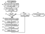
- FIG. 5 is a flowchart illustrating an embodiment of the techniques described above.
- processor 10 When processor 10 is placed in reset mode ( 90 ), processor 10 asserts Reset_Signal 50 ( 92 ). Asserting Reset_Signal 50 results in the asserting of Ext_Reset_Signal 24 as well ( 92 ). Once reset operations are completed, Reset_Signal 50 is cleared ( 94 ). When Reset_Signal 50 is cleared, reset logic 18 senses whether IM_Init 30 is asserted ( 96 ). When IM_Init 30 is not asserted, Ext_Reset_Signal 50 is cleared ( 108 ) and instruction fetching commences ( 110 ).
- Processor 10 optionally may disable interrupts ( 100 ) to prevent an interrupt handler from initiating fetching before loading of instruction memory 16 ( 102 ) is completed.
- IM_Init 30 is cleared ( 104 ).
- Interrupts, if disabled ( 100 ), are re-enabled ( 106 ).
- Ext_Reset_Signal 50 is cleared ( 108 ), which enables instruction fetch requests, and instruction fetching commences ( 110 ).
- the first fetched instruction may be, for example, the first instruction of a reset service routine.
- a number of embodiments of the invention have been described. For example, a method of resetting a processor has been described, in which fetch requests are disabled when the processor undergoes a reset, and remain disabled when the instruction memory is being loaded.
- the processor may be implemented in a variety of systems including general purpose computing systems, digital processing systems, laptop computers, personal digital assistants (PDA's) and cellular phones.
- PDA's personal digital assistants
- the resetting techniques discussed above may be readily used to improve processor performance.
- the processor may be coupled to a memory device, such as a FLASH memory device or a SRAM device, that stores an operating system and other software applications.
Abstract
Description
Claims (22)
Priority Applications (6)
| Application Number | Priority Date | Filing Date | Title |
|---|---|---|---|
| US09/738,082 US6789187B2 (en) | 2000-12-15 | 2000-12-15 | Processor reset and instruction fetches |
| PCT/US2001/047623 WO2002048872A2 (en) | 2000-12-15 | 2001-12-10 | Instruction loading after processor reset |
| CNB018207014A CN1279437C (en) | 2000-12-15 | 2001-12-10 | Extended processor reset |
| KR1020037007847A KR100571324B1 (en) | 2000-12-15 | 2001-12-10 | Instruction loading method and device after processor reset |
| JP2002550516A JP2004516545A (en) | 2000-12-15 | 2001-12-10 | Instruction loading after processor reset |
| TW090131101A TW539944B (en) | 2000-12-15 | 2001-12-14 | Extended processor reset |
Applications Claiming Priority (1)
| Application Number | Priority Date | Filing Date | Title |
|---|---|---|---|
| US09/738,082 US6789187B2 (en) | 2000-12-15 | 2000-12-15 | Processor reset and instruction fetches |
Publications (2)
| Publication Number | Publication Date |
|---|---|
| US20020078336A1 US20020078336A1 (en) | 2002-06-20 |
| US6789187B2 true US6789187B2 (en) | 2004-09-07 |
Family
ID=24966487
Family Applications (1)
| Application Number | Title | Priority Date | Filing Date |
|---|---|---|---|
| US09/738,082 Expired - Lifetime US6789187B2 (en) | 2000-12-15 | 2000-12-15 | Processor reset and instruction fetches |
Country Status (6)
| Country | Link |
|---|---|
| US (1) | US6789187B2 (en) |
| JP (1) | JP2004516545A (en) |
| KR (1) | KR100571324B1 (en) |
| CN (1) | CN1279437C (en) |
| TW (1) | TW539944B (en) |
| WO (1) | WO2002048872A2 (en) |
Families Citing this family (2)
| Publication number | Priority date | Publication date | Assignee | Title |
|---|---|---|---|---|
| KR100973263B1 (en) * | 2003-11-26 | 2010-07-30 | 주식회사 하이닉스반도체 | A memory device having initial values |
| KR100771877B1 (en) | 2006-07-21 | 2007-11-01 | 삼성전자주식회사 | Method and apparatus for processing command set protocol for preventing from malfunction |
Citations (28)
| Publication number | Priority date | Publication date | Assignee | Title |
|---|---|---|---|---|
| JPS55124803A (en) * | 1979-03-20 | 1980-09-26 | Toshiba Electric Equip Corp | Remote control unit |
| JPS5723151A (en) * | 1980-07-16 | 1982-02-06 | Fujitsu Ltd | Interruption processing system |
| US4429366A (en) * | 1981-04-09 | 1984-01-31 | Westinghouse Electric Corp. | Microprocessor-based load management terminal with reset |
| JPS62202234A (en) * | 1986-02-12 | 1987-09-05 | Fujitsu Ltd | Advance control system |
| US4698748A (en) * | 1983-10-07 | 1987-10-06 | Essex Group, Inc. | Power-conserving control system for turning-off the power and the clocking for data transactions upon certain system inactivity |
| US4729091A (en) | 1984-11-13 | 1988-03-01 | International Business Machines Corporation | Directing storage requests prior to address comparator initialization with a reference address range |
| US4791557A (en) * | 1985-07-31 | 1988-12-13 | Wang Laboratories, Inc. | Apparatus and method for monitoring and controlling the prefetching of instructions by an information processing system |
| US5057999A (en) * | 1988-08-05 | 1991-10-15 | Nippon Motorola, Ltd. | Microprocessor having a protection circuit to insure proper instruction fetching |
| US5168547A (en) * | 1989-12-29 | 1992-12-01 | Supercomputer Systems Limited Partnership | Distributed architecture for input/output for a multiprocessor system |
| US5226138A (en) * | 1990-11-27 | 1993-07-06 | Sun Microsystems, Inc. | Method for selectively transferring data instructions to a cache memory |
| US5576650A (en) * | 1994-04-25 | 1996-11-19 | Casio Computer Co., Ltd. | Reset circuit of electronic device |
| US5659712A (en) * | 1995-05-26 | 1997-08-19 | National Semiconductor Corporation | Pipelined microprocessor that prevents the cache from being read when the contents of the cache are invalid |
| US5680564A (en) * | 1995-05-26 | 1997-10-21 | National Semiconductor Corporation | Pipelined processor with two tier prefetch buffer structure and method with bypass |
| US5724533A (en) * | 1995-11-17 | 1998-03-03 | Unisys Corporation | High performance instruction data path |
| US5761469A (en) * | 1995-08-15 | 1998-06-02 | Sun Microsystems, Inc. | Method and apparatus for optimizing signed and unsigned load processing in a pipelined processor |
| US5850563A (en) * | 1995-09-11 | 1998-12-15 | International Business Machines Corporation | Processor and method for out-of-order completion of floating-point operations during load/store multiple operations |
| US5867684A (en) * | 1995-09-11 | 1999-02-02 | International Business Machines Corporation | Method and processor that permit concurrent execution of a store multiple instruction and a dependent instruction |
| US5897654A (en) * | 1995-02-10 | 1999-04-27 | International Business Machines Corporation | Method and system for efficiently fetching from cache during a cache fill operation |
| US6055625A (en) * | 1993-02-16 | 2000-04-25 | Fujitsu Limited | Pipeline computer with a scoreboard control circuit to prevent interference between registers |
| US6076161A (en) * | 1997-08-25 | 2000-06-13 | National Semiconductor Corporation | Microcontroller mode selection system and method upon reset |
| US6173396B1 (en) * | 1996-10-17 | 2001-01-09 | Robert Bosch Gmbh | Circuit configuration with a microprocessor |
| US6292883B1 (en) * | 1997-10-02 | 2001-09-18 | U.S. Philips Corporation | Converting program-specific virtual machine instructions into variable instruction set |
| US6330667B1 (en) | 1998-06-05 | 2001-12-11 | Micron Technology, Inc. | System for read only memory shadowing circuit for copying a quantity of rom data to the ram prior to initialization of the computer system |
| US6349072B1 (en) * | 1999-11-05 | 2002-02-19 | Matsushita Electric Industrial Co., Ltd. | Random access memory device |
| US6401197B1 (en) * | 1996-10-31 | 2002-06-04 | Mitsubishi Denki Kabushiki Kaisha | Microprocessor and multiprocessor system |
| US6581138B2 (en) * | 2000-02-29 | 2003-06-17 | Stmicroelectronics, Inc. | Branch-prediction driven instruction prefetch |
| US6665795B1 (en) * | 2000-10-06 | 2003-12-16 | Intel Corporation | Resetting a programmable processor |
| US6697931B1 (en) * | 1996-10-31 | 2004-02-24 | Stmicroelectronics Limited | System and method for communicating information to and from a single chip computer system through an external communication port with translation circuitry |
-
2000
- 2000-12-15 US US09/738,082 patent/US6789187B2/en not_active Expired - Lifetime
-
2001
- 2001-12-10 JP JP2002550516A patent/JP2004516545A/en active Pending
- 2001-12-10 WO PCT/US2001/047623 patent/WO2002048872A2/en active IP Right Grant
- 2001-12-10 KR KR1020037007847A patent/KR100571324B1/en active IP Right Grant
- 2001-12-10 CN CNB018207014A patent/CN1279437C/en not_active Expired - Fee Related
- 2001-12-14 TW TW090131101A patent/TW539944B/en not_active IP Right Cessation
Patent Citations (28)
| Publication number | Priority date | Publication date | Assignee | Title |
|---|---|---|---|---|
| JPS55124803A (en) * | 1979-03-20 | 1980-09-26 | Toshiba Electric Equip Corp | Remote control unit |
| JPS5723151A (en) * | 1980-07-16 | 1982-02-06 | Fujitsu Ltd | Interruption processing system |
| US4429366A (en) * | 1981-04-09 | 1984-01-31 | Westinghouse Electric Corp. | Microprocessor-based load management terminal with reset |
| US4698748A (en) * | 1983-10-07 | 1987-10-06 | Essex Group, Inc. | Power-conserving control system for turning-off the power and the clocking for data transactions upon certain system inactivity |
| US4729091A (en) | 1984-11-13 | 1988-03-01 | International Business Machines Corporation | Directing storage requests prior to address comparator initialization with a reference address range |
| US4791557A (en) * | 1985-07-31 | 1988-12-13 | Wang Laboratories, Inc. | Apparatus and method for monitoring and controlling the prefetching of instructions by an information processing system |
| JPS62202234A (en) * | 1986-02-12 | 1987-09-05 | Fujitsu Ltd | Advance control system |
| US5057999A (en) * | 1988-08-05 | 1991-10-15 | Nippon Motorola, Ltd. | Microprocessor having a protection circuit to insure proper instruction fetching |
| US5168547A (en) * | 1989-12-29 | 1992-12-01 | Supercomputer Systems Limited Partnership | Distributed architecture for input/output for a multiprocessor system |
| US5226138A (en) * | 1990-11-27 | 1993-07-06 | Sun Microsystems, Inc. | Method for selectively transferring data instructions to a cache memory |
| US6055625A (en) * | 1993-02-16 | 2000-04-25 | Fujitsu Limited | Pipeline computer with a scoreboard control circuit to prevent interference between registers |
| US5576650A (en) * | 1994-04-25 | 1996-11-19 | Casio Computer Co., Ltd. | Reset circuit of electronic device |
| US5897654A (en) * | 1995-02-10 | 1999-04-27 | International Business Machines Corporation | Method and system for efficiently fetching from cache during a cache fill operation |
| US5659712A (en) * | 1995-05-26 | 1997-08-19 | National Semiconductor Corporation | Pipelined microprocessor that prevents the cache from being read when the contents of the cache are invalid |
| US5680564A (en) * | 1995-05-26 | 1997-10-21 | National Semiconductor Corporation | Pipelined processor with two tier prefetch buffer structure and method with bypass |
| US5761469A (en) * | 1995-08-15 | 1998-06-02 | Sun Microsystems, Inc. | Method and apparatus for optimizing signed and unsigned load processing in a pipelined processor |
| US5867684A (en) * | 1995-09-11 | 1999-02-02 | International Business Machines Corporation | Method and processor that permit concurrent execution of a store multiple instruction and a dependent instruction |
| US5850563A (en) * | 1995-09-11 | 1998-12-15 | International Business Machines Corporation | Processor and method for out-of-order completion of floating-point operations during load/store multiple operations |
| US5724533A (en) * | 1995-11-17 | 1998-03-03 | Unisys Corporation | High performance instruction data path |
| US6173396B1 (en) * | 1996-10-17 | 2001-01-09 | Robert Bosch Gmbh | Circuit configuration with a microprocessor |
| US6401197B1 (en) * | 1996-10-31 | 2002-06-04 | Mitsubishi Denki Kabushiki Kaisha | Microprocessor and multiprocessor system |
| US6697931B1 (en) * | 1996-10-31 | 2004-02-24 | Stmicroelectronics Limited | System and method for communicating information to and from a single chip computer system through an external communication port with translation circuitry |
| US6076161A (en) * | 1997-08-25 | 2000-06-13 | National Semiconductor Corporation | Microcontroller mode selection system and method upon reset |
| US6292883B1 (en) * | 1997-10-02 | 2001-09-18 | U.S. Philips Corporation | Converting program-specific virtual machine instructions into variable instruction set |
| US6330667B1 (en) | 1998-06-05 | 2001-12-11 | Micron Technology, Inc. | System for read only memory shadowing circuit for copying a quantity of rom data to the ram prior to initialization of the computer system |
| US6349072B1 (en) * | 1999-11-05 | 2002-02-19 | Matsushita Electric Industrial Co., Ltd. | Random access memory device |
| US6581138B2 (en) * | 2000-02-29 | 2003-06-17 | Stmicroelectronics, Inc. | Branch-prediction driven instruction prefetch |
| US6665795B1 (en) * | 2000-10-06 | 2003-12-16 | Intel Corporation | Resetting a programmable processor |
Also Published As
| Publication number | Publication date |
|---|---|
| CN1481528A (en) | 2004-03-10 |
| CN1279437C (en) | 2006-10-11 |
| US20020078336A1 (en) | 2002-06-20 |
| JP2004516545A (en) | 2004-06-03 |
| WO2002048872A2 (en) | 2002-06-20 |
| WO2002048872A3 (en) | 2003-01-16 |
| KR100571324B1 (en) | 2006-04-17 |
| TW539944B (en) | 2003-07-01 |
| KR20030059338A (en) | 2003-07-07 |
Similar Documents
| Publication | Publication Date | Title |
|---|---|---|
| JP3688270B2 (en) | Stop processor | |
| US6823448B2 (en) | Exception handling using an exception pipeline in a pipelined processor | |
| US5822602A (en) | Pipelined processor for executing repeated string instructions by halting dispatch after comparision to pipeline capacity | |
| JP2858140B2 (en) | Pipeline processor device and method | |
| US7356717B2 (en) | Information processing apparatus with central processing unit and main memory having power saving mode, and power saving controlling method | |
| US6760835B1 (en) | Instruction branch mispredict streaming | |
| WO1995008801A1 (en) | Execution of data processing instructions | |
| US7272705B2 (en) | Early exception detection | |
| US6665795B1 (en) | Resetting a programmable processor | |
| JP3737083B2 (en) | Multicycle instruction | |
| US6842812B1 (en) | Event handling | |
| US6789187B2 (en) | Processor reset and instruction fetches | |
| US6721878B1 (en) | Low-latency interrupt handling during memory access delay periods in microprocessors | |
| JPH07311686A (en) | Computer system and method for generation and processing of system management interrupt in it | |
| US20040128484A1 (en) | Method and apparatus for transparent delayed write-back | |
| US7124285B2 (en) | Peak power reduction when updating future file | |
| JPH07182165A (en) | Processing method/device for instruction with committing condition | |
| JPS61269735A (en) | Instruction queue control system of electronic computer | |
| JP2926975B2 (en) | Program control unit | |
| JP2885548B2 (en) | Pipeline control method |
Legal Events
| Date | Code | Title | Description |
|---|---|---|---|
| AS | Assignment |
Owner name: INTEL CORPORATION, CALIFORNIA Free format text: ASSIGNMENT OF ASSIGNORS INTEREST;ASSIGNORS:SINGH, RAVI P.;ROTH, CHARLES P.;KOLAGOTLA, RAVI;AND OTHERS;REEL/FRAME:011368/0818;SIGNING DATES FROM 20001106 TO 20001107 Owner name: ANALOG DEVICES, INC., MASSACHUSETTS Free format text: ASSIGNMENT OF ASSIGNORS INTEREST;ASSIGNORS:SINGH, RAVI P.;ROTH, CHARLES P.;KOLAGOTLA, RAVI;AND OTHERS;REEL/FRAME:011368/0818;SIGNING DATES FROM 20001106 TO 20001107 |
|
| STCF | Information on status: patent grant |
Free format text: PATENTED CASE |
|
| FEPP | Fee payment procedure |
Free format text: PAYOR NUMBER ASSIGNED (ORIGINAL EVENT CODE: ASPN); ENTITY STATUS OF PATENT OWNER: LARGE ENTITY Free format text: PAYER NUMBER DE-ASSIGNED (ORIGINAL EVENT CODE: RMPN); ENTITY STATUS OF PATENT OWNER: LARGE ENTITY |
|
| AS | Assignment |
Owner name: ANALOG DEVICES, INC., MASSACHUSETTS Free format text: ASSIGNMENT OF ASSIGNORS INTEREST;ASSIGNOR:INTEL CORPORATION;REEL/FRAME:018891/0599 Effective date: 20061108 |
|
| FPAY | Fee payment |
Year of fee payment: 4 |
|
| FPAY | Fee payment |
Year of fee payment: 8 |
|
| FPAY | Fee payment |
Year of fee payment: 12 |