US7774666B2 - Analyzer - Google Patents
Analyzer Download PDFInfo
- Publication number
- US7774666B2 US7774666B2 US11/866,595 US86659507A US7774666B2 US 7774666 B2 US7774666 B2 US 7774666B2 US 86659507 A US86659507 A US 86659507A US 7774666 B2 US7774666 B2 US 7774666B2
- Authority
- US
- United States
- Prior art keywords
- scan
- analyzer
- actual operation
- data
- operable
- Prior art date
- Legal status (The legal status is an assumption and is not a legal conclusion. Google has not performed a legal analysis and makes no representation as to the accuracy of the status listed.)
- Expired - Fee Related, expires
Links
Images


Classifications
-
- G—PHYSICS
- G01—MEASURING; TESTING
- G01R—MEASURING ELECTRIC VARIABLES; MEASURING MAGNETIC VARIABLES
- G01R31/00—Arrangements for testing electric properties; Arrangements for locating electric faults; Arrangements for electrical testing characterised by what is being tested not provided for elsewhere
- G01R31/28—Testing of electronic circuits, e.g. by signal tracer
- G01R31/317—Testing of digital circuits
- G01R31/3181—Functional testing
- G01R31/3185—Reconfiguring for testing, e.g. LSSD, partitioning
- G01R31/318533—Reconfiguring for testing, e.g. LSSD, partitioning using scanning techniques, e.g. LSSD, Boundary Scan, JTAG
- G01R31/318536—Scan chain arrangements, e.g. connections, test bus, analog signals
-
- G—PHYSICS
- G01—MEASURING; TESTING
- G01R—MEASURING ELECTRIC VARIABLES; MEASURING MAGNETIC VARIABLES
- G01R31/00—Arrangements for testing electric properties; Arrangements for locating electric faults; Arrangements for electrical testing characterised by what is being tested not provided for elsewhere
- G01R31/28—Testing of electronic circuits, e.g. by signal tracer
- G01R31/317—Testing of digital circuits
- G01R31/3181—Functional testing
- G01R31/3185—Reconfiguring for testing, e.g. LSSD, partitioning
- G01R31/318533—Reconfiguring for testing, e.g. LSSD, partitioning using scanning techniques, e.g. LSSD, Boundary Scan, JTAG
- G01R31/318544—Scanning methods, algorithms and patterns
Definitions
- the present invention relates to analyzers and in particular to an analyzer having a scan test function.
- FFs flip-flops
- the FFs function as a shift register when a scan test is performed, apart from ordinary logic used at the time of actual operation. This makes it possible to set predetermined values in the FFs inside the circuit from, for example, input terminals for test without being affected by the internal logic in the circuit, when the circuit is in a mode to operate a scan test (hereinafter referred to as scan mode).
- scan mode a mode to operate a scan test
- FIG. 1 is a block diagram illustrating the configuration of the conventional analyzer.
- the analyzer 900 illustrated in FIG. 1 has scan paths 901 a and 901 b , selectors 904 a and 904 b , and a dummy FF (flip-flop) 906 .
- the scan paths 901 a and 901 b are circuits for scan test, integrated into an actual operation circuit.
- the scan paths 901 a and 901 b operate as a shift register in the scan mode, and perform a shift operation in accordance with clocks 902 .
- the number of stages in the FFs therein is smaller than that of the FFs in the scan path 901 a.
- the dummy FF 906 is an FF that is not used in actual operation.
- the number of stages in the FFs in the scan path 901 a is equal to the sum of that of the FFs in the scan path 901 b and that of the dummy FF 906 .
- the selector 904 a selects a scan path output 903 a , which is an output from the scan path 901 a , or a scan path input 905 a , and then connects the selected one to the input of the scan path 901 a .
- the selector 904 b selects a scan path output 903 b , which is an output from the scan path 901 b , or a scan path input 905 b , and then connects the selected one to the input of the scan path 901 b.
- the selectors 904 a and 904 b select the scan path outputs 903 a and 903 b , respectively.
- the scan paths 901 a and 901 b each performs shift operation whenever one of the clocks 902 is inputted thereto, so that values of the FFs in the internal circuit (i.e., values of the FFs in the scan paths 901 a and 901 b ) are sequentially outputted as the scan path outputs 903 a and 903 b , respectively.
- values of the FFs included in the scan paths 901 a and 901 b become the same values as those when the scan test starts (when the end of the actual operation mode). In this manner, it becomes possible to carry out actual operation continuously after the scan mode. Furthermore, providing the dummy FF 906 makes it possible that, although the analyzer has scan paths in which the numbers of stages in the FFs therein are different from each other, values of the FFs included in the scan paths are returned to the values when the scan test starts, by using the same number of clocks.
- the object of the present invention is to provide an analyzer which can restore the values of the FFs to the values when the scan test starts, so as to prevent increase in circuit size.
- the analyzer is an analyzer having a scan test function, including: scan paths, each including flip-flops which functions as a shift register when a scan test is performed; and a switching unit which switches between a first connection state, and a second connection state in which the scan paths are connected in series and an output from the scan path at the last stage is connected to an input of the scan path at the first stage.
- the plurality of scan paths can be connected in series by the switching unit, so that the scan paths can be handled as a large shift register.
- the scan paths form a feedback.
- the individual scan paths can be connected to each other and the connected scan paths can be regarded as a large scan path, whereby the inputs and the outputs can be respectively unified. This makes it possible to decrease the number of paths for inputting and outputting data in and from the scan paths.
- the switching unit may switch between the first connection state and the second connection state, the first connection state being a state in which to the input of each of the scan paths connected is a signal to be written in the scan path at the time of the scan test.
- the switching unit can select data to be written in each of the scan paths, thereby writing the data in the FFs included in each of the scan paths. Furthermore, data read out by the scan test operation can again be written, thereby reproducing the state of the circuit any number of times when the data is read out.
- the analyzer may further include a data converting unit which replaces predetermined data with the output from the scan path at the last stage, in which the switching unit switches between the first connection state and the second connection state, the second connection state being a state in which the scan paths are connected in series and the data replaced by the data converting unit is connected to the input of the scan path at the first stage.
- a data converting unit which replaces predetermined data with the output from the scan path at the last stage, in which the switching unit switches between the first connection state and the second connection state, the second connection state being a state in which the scan paths are connected in series and the data replaced by the data converting unit is connected to the input of the scan path at the first stage.
- the data converting unit makes it possible to change the value of any one of the FFs on the data taken out from the scan path outputs. As a result of this, it can be observed what change is caused in the operation of specific one of the FFs, the state of the specific one being changed at the time of the analysis.
- the data converting unit may includes a memory unit operable to store information for specifying each of the flip-flops included in the scan paths, and the data converting unit replaces data stored in the flip-flops included in the scan paths based on the information stored in the memory unit.
- the data converting unit can write data in designated one of the FFs by use of information for specifying one of the FFs included in the scan paths, the specifying information being stored in the memory unit.
- the analyzer may further include: a memory unit in which data used at the time of actual operation is stored; and a memory controlling unit which controls the operation of the memory unit independently of the scan operation of the scan paths at the time of the scan test.
- the memory controlling unit can hold data in the memory unit by performing refresh operation in the scan test. In this way, the memory unit can hold data when the scan test starts (i.e., when the actual operation ends) when the operation mode is shifted to the actual operation mode.
- the analyzer may further include: a first memory unit in which data used at the time of actual operation is stored; and a second memory unit which stores the data stored by the first memory unit when the scan test starts.
- the data in the first memory unit used in the actual operation can be stored in the second memory unit and the data in the second memory unit can be returned into the first memory unit before returning to the actual operation.
- the first memory unit can hold the data when the scan test started when the operation mode is again shifted to the actual operation mode.
- the scan paths may include a first scan path and a second scan path
- the analyzer may include: a first functional block including the first scan path; and a second functional block including the second scan path, and operating asynchronously with the first functional block at the time of actual operation
- the first functional block may include a data transmitting unit which transmits data to the second functional block
- the second functional block may include a data receiving unit which generates an acknowledge signal for notifying the first functional block that the data is received when properly receives the data from the data transmitting unit
- the data receiving unit transmits the acknowledge signal to the first functional block when the operation mode performed by the analyzer is shifted to actual operation and the state of the second functional block turns into a data-receivable state.
- the data receiving unit in the second functional block transmits the acknowledge signal for notifying that the data receiving unit can receive data to the first functional block.
- the data transmitting unit in the first functional block receives the acknowledge signal from the second functional block
- the data transmitting unit can understand that the second functional block is in a data-receivable state.
- the scan paths may include a first scan path and a second scan path
- the analyzer may further include: a first functional block including the first scan path, and operating in accordance with a first clock at the time of actual operation; a second functional block including the second scan path, and operating in accordance with a second clock that is asynchronous with the first clock at the time of the actual operation; a phase difference detecting unit which detects a phase difference between the first clock and the second clock when the actual operation is shifted to the scan test; a phase difference holding unit which holds the phase difference detected by the phase difference detecting unit; and a delay controlling unit which delays, when the operation mode performed by the analyzer is returned from the scan test to the actual operation, to at least one of the first clock and the second clock, thereby making the phase difference between the first clock and the second clock equal to the phase difference held by the phase difference holding unit.
- the phases supplied to the individual functional blocks can be made to phases when the actual operation ends.
- the following can be prevented in the functional blocks having the asynchronous clock systems: when the operation mode is returned from the scan test mode to the actual operation mode, a malfunction (duplicate transmission of data or non-transmission of data) is generated.
- the scan paths may include a first scan path and a second scan path
- the analyzer may further include: a first functional block including the first scan path and operating in accordance with a first clock at the time of actual operation; a second functional block including the second scan path and operating in accordance with a second clock that is asynchronous with the first clock at the time of the actual operation; a first selecting unit which selects the first clock or a third clock and supply the selected clock to the first functional block; and a second selecting unit which selects the second clock or a fourth clock that is synchronous with the third clock and supply the selected clock to the second functional block.
- the analyzer may further includes: an oscillating unit which oscillates a clock used at the time of actual operation; and an oscillation controlling unit which stops the oscillation of the oscillating unit when the operation mode performed by the analyzer is shifted from the actual operation to the scan test.
- the oscillation of the oscillating unit is stopped when the actual operation is stopped, and the oscillating unit is again operated when the operation mode is again returned to the actual operation mode. This makes it possible to decrease the generation of noises due to the oscillation of the oscillating unit at the time of the scan test. Furthermore, the power consumption in the scan test can be reduced.
- the analyzer may further includes: a clock controlling unit which waits for the stabilization of the oscillation of the oscillating unit and resume the supply of the clock used in the actual operation when the operation mode performed by the analyzer is returned from the scan test to the actual operation.
- a clock controlling unit which waits for the stabilization of the oscillation of the oscillating unit and resume the supply of the clock used in the actual operation when the operation mode performed by the analyzer is returned from the scan test to the actual operation.
- the operation mode can be returned to the actual operation mode in accordance with stable clocks by waiting for the stabilization of the oscillation of the oscillating unit.
- the occurrence of malfunction can be prevented.
- the analyzer may further includes: an external data acquiring unit which acquires data from an external device at the time of actual operation; and an external device controlling unit which stops the external device at the time of the scan test and resume the operation of the external device when the operation mode performed by the analyzer is returned from the scan test to the actual operation.
- the operation of the external device can be stopped when the actual operation is stopped to perform the scan test, and the operation of the external device is resumed when the operation mode is returned to the actual operation mode, thereby continuing normal operation when the operation mode is returned to the actual operation mode.
- the analyzer may further includes: an image data outputting unit which outputs image data at the time of actual operation, and output the image data when the actual operation ends, as still image data, at the time of the scan test.
- an external display device displays an image when the actual operation ends on the basis of the image data outputted from the image data outputting unit. This makes it possible to avoid a problem that, in the case of conducting analysis while seeing images, the output of the image data is stopped, thereby stopping the synchronizing signal for the display so that no image is outputted.
- the analyzer may further includes a synchronization controlling unit which resumes the actual operation in accordance with the timing based on a synchronizing signal for the image data outputting unit when the operation mode performed by the analyzer is returned from the scan test to the actual operation.
- the operation mode can be returned to the actual operation mode at the same display timing as when the accrual operation is stopped. This makes it possible to avoid a situation in which a lag is generated in the synchronization of images when the operation mode is returned from the scan test mode to the actual operation mode.
- the scan paths are respectively formed in different functional blocks, and the analyzer further includes a mode switching unit which controls the scan test and actual operation in each of the scan paths independently.
- the scan paths operate independently of each other in the individual functional blocks. This makes it possible to stop the actual operation only in specific one of the functional blocks to perform the scan test. Moreover, it is possible to operate only the scan path having a specific function in the actual operation mode, thereby reading out data in the internal circuit.
- the analyzer may further include a detecting unit which detects an internal failure at the time of actual operation and to output an interrupt signal for notifying the outside of the failure.
- the detecting unit outputs an interrupt signal to the outside of the analyzer when a target phenomenon such as an internal failure occurs.
- a target phenomenon such as an internal failure
- the analyzer may further include a mode switching unit which stops the actual operation in accordance with a signal from the outside and perform the scan test.
- the actual operation mode is stopped to shift the operation mode to the scan test mode. This makes it possible to stop the actual operation of the analyzer at the timing of occurrence of a failure in an externally-connected device or the like, thereby performing the scan test.
- the analyzer may further include a selecting signal generating unit which generates a selecting signal for selecting a specific one out of the flip-flops, in which when each of the flip-flops is according to the selecting signal, the selected flip-flop outputs data held therein to the flip-flop at the stage immediately after the selected flip-flop by use of the scan path, and when each of the flip-flops is not according to the selecting signal, the unselected flip-flop outputs data outputted from the flip-flop at the stage immediately before the unselected flip-flop to the flip-flop at the stage immediately after the unselected flip-flop.
- a selecting signal generating unit which generates a selecting signal for selecting a specific one out of the flip-flops, in which when each of the flip-flops is according to the selecting signal, the selected flip-flop outputs data held therein to the flip-flop at the stage immediately after the selected flip-flop by use of the scan path, and when each of the flip-flops is not according to the selecting signal, the unselected flip-flop outputs data outputted from
- a specific FF can be selected and data in the selected FF can be read out. Moreover, an increase in the circuit scale can be prevented by use of the scan paths.
- the analyzer may further include: a determining unit which determines whether or not data outputted from one or more of the scan paths matches predetermined data at the time of actual operation; and a mode switching unit stops the actual operation and perform the scan test when the determining unit determines that the data matches the predetermined data.
- the operation mode can be shifted from the actual operation mode to the scan test mode in accordance with data held in specific one of the FFs. This makes it possible to stop the actual operation and conduct analysis at the timing at which the internal state turns into a predetermined state.
- the selecting signal generated by the selecting signal generating unit may includes a first selecting signal and a second selecting signal, and each of the flip-flops is selected on the basis of the logical sum of the first selecting signal and the second selecting signal.
- a specific FF can be specified in accordance with the selecting signals in the actual operation mode, thereby specifying the FF with the smaller number of wirings.
- an analyzer having a scan test function may include: scan paths, each including flip-flops which function as a shift register when a scan test is performed, a switching unit which switches between a first connection state, and a second connection state in which an output from each of the scan paths is connected to the input of the scan path, and a clock controlling unit which supplies clocks to each of the scan paths, the clocks numbering as many as the number of stages in the flip-flops included in the scan path during an scan operation in which data in all of the flip-flops included in the scan paths at the time of the scan test is read out.
- the clock controlling unit outputs, to each of the scan paths, the clocks the number of which is equal to the number of stages in the FFs in the scan paths.
- the analyzer may further include a parallel-serial converting unit which converts outputs from the scan paths to a serial signal.
- outputs from the scan paths can be converted to serial signals.
- the number of terminals for outputting data can be decreased. For example, when the actual operation is stopped to perform the scan test, the number of terminals for reading out data may be small; therefore, data can be read out while many of all the terminals keep a terminal state in the actual operation mode.
- the analyzer may further include a serial-parallel converting unit which converts a serial signal to parallel signals, in which the switching unit switches between the first connection state which is a first connection state in which the parallel signals converted by the serial-parallel converting unit are connected to the inputs of the scan paths, and the second connection state.
- a serial-parallel converting unit which converts a serial signal to parallel signals, in which the switching unit switches between the first connection state which is a first connection state in which the parallel signals converted by the serial-parallel converting unit are connected to the inputs of the scan paths, and the second connection state.
- the serial signal inputted from the outside are converted to parallel signals, and then the parallel signals are assigned to the inputs of each of the scan paths.
- the number of terminals used to input data into the scan paths can be decreased. For example, when the actual operation is stopped to perform the scan test, the number of terminals for writing data may be small; therefore, data can be written while many terminals keep a terminal state in the actual operation mode.
- an analyzer may include: a first analyzing device; a second analyzing device having the same circuit configuration as the first analyzing device; and an activating unit which activates the first analyzing device and the second analyzing device at different timings; the mode switching unit in the second analyzing device stops the actual operation and perform the scan test in accordance with the interrupt signal outputted from the detecting unit in the first analyzing device.
- the actual operation of the second analyzing device is stopped by the aid of an interrupt signal from the first analyzing device, so that the operation mode is shifted to the scan test mode. Since the first and second analyzing devices have the same circuit configuration, the internal state of the second analyzing device, which starts to operate later than the first analyzing device, becomes a state before the failure occurs. In short, the state of the internal circuit before the occurrence of the failure can be analyzed by reading out data in the scan paths in the second analyzing device.
- the activating unit may activate the first analyzing device and the second analyzing device at different timings by making the timing of releasing a reset signal for resetting the operation of the first analyzing device different from the timing of releasing a reset signal for resetting the operation of the second analyzing device.
- wiring for clocks and so on can be shared by making the timing of reset signals different for booting the individual analyzing devices.
- the number of the wirings can be reduced.
- the present invention makes it possible to return values in the FFs to values when the scan test starts.
- an analyzer wherein an increase in the circuit scale is prevented can be provided.
- FIG. 1 shows a configuration of a conventional analyzer
- FIG. 2 shows a configuration of an analyzer according to a first embodiment of the present invention
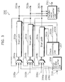
- FIG. 3 is shows a configuration of an analyzer according to a second embodiment of the present invention.
- FIG. 4 shows a configuration of an analyzer according to a third embodiment of the present invention.
- FIG. 5 shows a configuration of an analyzer according to a fourth embodiment of the present invention.
- FIG. 6 shows a configuration of an analyzer according to a fifth embodiment of the present invention.
- FIG. 7 shows a configuration of an analyzer according to a sixth embodiment of the present invention.
- FIG. 8 shows a configuration of an analyzer according to a seventh embodiment of the present invention.
- FIG. 9 shows a configuration of a scan flip-flop in the analyzer according to the seventh embodiment of the present invention.
- An analyzer has a mode in which scan paths are connected in series in a scan test operation so as to form a single shift register.
- the analyzer also has a function of looping an output from the scan paths connected in series to the input of the shift register.
- FIG. 2 is a block diagram illustrating the configuration of the analyzer according to the first embodiment.
- the analyzer 100 illustrated in FIG. 2 is a circuit which is integrated into, for example, a semiconductor integrated circuit and has a scan function.
- the analyzer 100 includes scan paths 101 a , 101 b and 101 c , and selectors 104 a , 104 b and 104 c.
- the scan paths 101 a , 101 b and 101 c are scan test circuits integrated into an actual operation circuit, and each includes FFs.
- the FFs included in each of the scan paths 101 a , 101 b and 101 c function as a shift register in a scan mode (in a mode in which scan test operation is performed).
- the scan path 101 a performs a shift operation in accordance with clocks 102 in the scan mode to sequentially output data in the FFs included in the scan path 101 a as a scan path output 103 a .
- the scan path 101 b performs a shift operation in accordance with the clocks 102 in the scan mode to sequentially output data in the FFs included in the scan path 101 b as a scan path output 103 b .
- the scan path 101 c performs a shift operation in accordance with the clocks 102 in the scan mode to sequentially output data in the FFs included in the scan path 101 c as a scan path output 103 c.
- the clocks 102 are clocks used for the shift operation of the scan paths 101 a , 101 b and 101 c when a scan test is performed, and are inputted, for example, from the outside of a semiconductor device including the analyzer 100 .
- the scan path outputs 103 a , 103 b and 103 c are signals outputted to the outside of the semiconductor integrated circuit including the analyzer 100 .
- the selector 104 a selects one of the scan path output 103 c and a scan path input 105 a , and connects the selected one to the input of the scan path 101 a .
- the selector 101 b selects one of the scan path output 103 a and a scan path input 105 b , and connects the selected one to the input of the scan path 101 b .
- the selector 104 c selects one of the scan path output 103 b and a scan path input 105 c , and connects the selected one to the input of the scan path 101 c .
- the selectors 104 a , 104 b and 104 c switch between the following first and second connection states: a first connection state where the scan path inputs 105 a , 105 b and 105 c , which are signals respectively to be written in the scan paths 101 a , 101 b and 101 c when a scan test is performed, are respectively connected to the inputs of the scan paths 101 a , 101 b and 101 c ; and a second connection state where the scan paths 101 a , 101 b and 101 c are connected in series, and the scan path output 103 c , which is an output from the scan path 101 c of the last stage, is connected to the input of the scan path 101 a of the first stage.
- the scan path inputs 105 a , 105 b and 105 c are, for example, signals inputted from the outside of the semiconductor integrated circuit including the analyzer 100 .
- An actual operation mode is a mode in which an ordinary operation of the semiconductor integrated circuit including the analyzer 100 is performed.
- the FFs included in the scan paths 101 a , 101 b and 101 c are connected to the circuit for actual operation, and operate as FFs in the actual operation circuit.
- the FFs included in each of the scan paths 101 a , 101 b and 101 c operate as a shift register.
- the scan paths 101 a , 101 b and 101 c perform shift operations through the clocks 102 .
- the scan mode includes a first scan mode and a second scan mode.
- the selectors 104 a , 104 b and 104 c select the scan path inputs 105 a , 105 b and 105 c , respectively.
- the scan path inputs 105 a , 105 b and 105 c are sequentially shifted in the scan paths 101 a , 101 b and 101 c , respectively, and then held in the FFs included in the scan paths 101 a , 101 b and 101 c , respectively.
- data held in the FFs included in the scan paths 101 a , 101 b and 101 c are sequentially shifted in the scan paths 101 a , 101 b and 101 c , respectively, and then outputted as the scan path outputs 103 a , 103 b and 103 c , respectively.
- data from the outside can be set into the FFs included in the scan paths 101 a , 101 b and 101 c .
- the scan mode starts (i.e., when the actual operation mode ends)
- data held in the FFs included in the scan paths 101 a , 101 b and 101 c can be outputted to the outside.
- the selectors 104 a , 104 b and 104 c select the scan path outputs 103 c , 103 a and 103 b , respectively.
- the output from the scan path 101 a is connected to the input of the scan path 101 b
- the output from the scan path 101 b is connected to the input of the scan path 101 c
- the output from the scan path 101 c is connected to the input of the scan path 101 a .
- the scan paths 101 a , 101 b and 101 c function as a single shift register so as to form a loop.
- the data in the FFs included in the scan paths 101 a , 101 b and 101 c are sequentially outputted as the scan path output 103 c when one of the clocks 102 is inputted to the analyzer. Specifically, when one of the clocks 102 is inputted to the analyzer, the data is sequentially outputted from the FF of the last stage in the scan path 101 c up to the FF of the first stage in the scan path 101 c . Next, the data in the FF of the last stage in the scan path 101 b to the FF of the first stage in the scan path 101 b are sequentially outputted. Then, the data in the FF of the last stage in the scan path 101 a to the FF of the first stage in the scan path 101 a are sequentially outputted.
- the analyzer 100 makes it possible that the data held in all the FFs included in the scan paths 101 a , 101 b and 101 c are respectively outputted as the scan path output 103 c when the scan mode starts (i.e., when the actual operation mode ends) by inputting the clocks 102 the number of which is equal to the total number of stages in all the FFs included in the scan paths 101 a , 101 b and 101 c to the analyzer.
- the conventional analyzer 900 illustrated in FIG. 1 When the numbers of stages in the FFs in the scan paths are different from each other, it is necessary for the conventional analyzer 900 illustrated in FIG. 1 to have the dummy FF 906 in order to perform the actual operation continuously after the scan test.
- the analyzer 100 according to the first embodiment of the present invention no dummy FF is required even when the numbers of the stages in the FFs in the scan paths 101 a , 101 b and 101 c are different from each other.
- an increase in the circuit scale can be prevented.
- the numbers of clocks supplied to individual scan paths are controlled when a scan test is performed.
- the analyzer has a function of looping outputs from the scan paths to inputs thereof. This makes it possible that even when the numbers of stages in the FFs in the scan paths are different from each other, data held in the FFs in the scan paths are returned to the state when the scan test starts, by inputting clocks the numbers of which are equal to the numbers of stages in the individual FFs. Thus, after the scan operation, the actual operation can be continuously performed.
- FIG. 3 is a block diagram illustrating the configuration of the analyzer according to the second embodiment of the present invention.
- the analyzer 200 illustrated in FIG. 3 is a circuit which is integrated into, for example, a semiconductor integrated circuit and has a scan function.
- the analyzer 200 includes scan paths 201 a , 201 b and 201 c , selectors 204 a , 204 b and 204 c , a clock controlling unit 207 , a serial-parallel converter unit 208 , and a parallel-serial converter unit 209 .
- the scan paths 201 a , 201 b and 201 c are scan test circuits integrated into an actual operation circuit, and each includes FFs.
- the FFs included in each of the scan paths 201 a , 201 b and 201 c function as a shift register in the scan mode.
- the scan path 201 a performs a shift operation in accordance with clocks 202 a when a scan test is performed to sequentially output data in the FFs included in the scan path 201 a as a scan path output 203 a .
- the scan path 201 b performs a shift operation in accordance with clocks 202 b in the scan test mode to sequentially output data in the FFs included in the scan path 201 b as a scan path output 203 b .
- the scan path 201 c performs a shift operation in accordance with clocks 202 c in the scan test mode to sequentially output data in the FFs included in the scan path 201 c as a scan path output 203 c .
- the scan path outputs 203 a , 203 b and 203 c are, for example, signals outputted to the outside of the semiconductor integrated circuit including the analyzer 200 .
- the selector 204 a selects one of the scan path output 203 a , a scan path input 205 a and a parallel input 206 a , and connects the selected one to the input of the scan path 201 a .
- the selector 204 b selects one of the scan path output 203 b , a scan path input 205 b and a parallel input 206 b , and connects the selected one to the input of the scan path 201 b .
- the selector 204 c selects one of the scan path output 203 c , a scan path input 205 c and a parallel input 206 c , and connects the selected one to the input of the scan path 201 c .
- the selectors 204 a , 204 b and 204 c switch the following first, second and third connection states from each other: a first connection state in which the scan path inputs 205 a , 205 b and 205 c , which are signals respectively written, when a scan test is performed, in the scan paths 201 a , 201 b and 201 c that are respectively connected to the inputs of the scan paths 201 a , 201 b and 201 c ; a second connection state in which the scan path outputs 203 a , 203 b and 203 c , which are outputs from the scan paths 201 a , 201 b and 201 c , respectively, are connected to the inputs of the scan paths 201 a , 201 b and 201 c , respectively; and a third connection state in which the parallel inputs 206 a , 206 b and 206 c are connected to the inputs of the scan paths 201 a
- the scan path inputs 205 a , 205 b and 205 c are signals set in the FFs in the scan paths 201 a , 201 b and 201 c , respectively, in the scan mode.
- the scan path inputs 201 a , 201 b and 201 c are signals inputted from, for example, the outside of the semiconductor integrated circuit including the analyzer 200 .
- the clock controlling unit 207 outputs clocks 202 a , 202 b and 202 c used in shift operations of the scan paths 201 a , 201 b and 201 c , respectively, in the scan mode.
- the clock controlling unit 207 outputs the clocks 202 a , 202 b and 202 c the numbers of which are respectively equal to the numbers of stages in the FFs included in the scan paths 201 a , 201 b and 201 c .
- the clock controlling unit 207 supplies, to the scan path 201 a , the clocks 202 a the number of which is equal to the number of stages in the FFs included in the scan path 201 a , supplies, to the scan path 201 b , the clocks 202 b the number of which is equal to the number of stages in the FFs included in the scan path 201 b , and supplies, to the scan path 201 c , the clocks 202 c the number of which is equal to the number of stages in the FFs included in the scan path 201 c .
- the clock controlling unit 207 holds the numbers of stages in the FFs in the scan paths 201 a , 201 b and 201 c , respectively, and outputs the clocks the numbers of which are equal to the numbers of stages in the FFs included in the scan paths 201 a , 201 b and 201 c , respectively, on the basis of reference clocks inputted from the outside. Thereafter, until the unit 207 outputs clocks the number of which is equal to the number of stages in the FFs included in the scan path that includes an FF in which the number of stages is the largest, out of the scan paths 201 a , 201 b and 201 c , the clock controlling unit 207 masks clocks so as to output no clock.
- the serial-parallel converter unit 208 performs serial-parallel conversion to a serial input 210 , which is a serial signal, to output parallel inputs 206 a , 206 b and 206 c , which are parallel signals of three bits.
- the parallel-serial converter unit 209 performs parallel-serial conversion to the scan path outputs 203 a , 203 b and 203 c , which are parallel signals of 3 bits, to output the serial output 211 , which is a serial signal.
- the serial input 210 is serial data set in the FFs included in the scan paths 201 a , 201 b and 201 c in the scan mode (specifically, in a third scan mode, which will be described later).
- the serial input 210 is, for example, a signal inputted from the outside of the semiconductor integrated circuit including the analyzer 200 .
- the serial outputs 211 are, for example, signals to be outputted to the outside of the semiconductor integrated circuit including the analyzer 200 .
- An actual operation mode is a mode in which a normal operation of the semiconductor integrated circuit including the analyzer 200 is performed.
- the FFs included in the scan paths 201 a , 201 b and 201 c are connected to the circuit for actual operation, and operate as FFs in the actual operation circuit.
- the FFs included in each of the scan paths 201 a , 201 b and 201 c operate as a shift register.
- the scan paths 201 a , 210 b and 210 c perform shift operations through the clocks 202 a , 202 b and 202 c , respectively.
- the scan mode includes a first scan mode, a second scan mode and a third scan mode.
- the selectors 204 a , 204 b and 204 c select the scan path inputs 205 a , 205 b and 205 c , respectively.
- the scan path inputs 205 a , 205 b and 205 c are sequentially shifted in the scan paths 201 a , 201 b and 201 c , respectively, and then held in the FFs included in the scan paths 201 a , 201 b and 201 c , respectively.
- data held in the FFs included in the scan paths 201 a , 201 b and 201 c are sequentially shifted in the scan paths 201 a , 201 b and 201 c , respectively, and then outputted as the scan path outputs 203 a , 203 b and 203 c , respectively.
- data from the outside can be set in the FFs included in the scan paths 201 a , 201 b and 201 c .
- data held in the FFs included in the scan paths 201 a , 201 b and 201 c can be outputted to the outside.
- the selectors 204 a , 204 b and 204 c select the scan path outputs 203 a , 203 b and 203 c , respectively.
- each of the scan paths 201 c , 201 a and 201 b forms a loop between the output and the input.
- the data in the FFs included in the scan paths 201 a , 201 b and 201 c is sequentially outputted as the scan path outputs 203 a , 203 b and 203 c , respectively, when one of the clocks 202 a , one of the clocks 202 b and one of the clocks 202 c are inputted, respectively.
- the data in the FF of the last stage in the scan path 201 a to the FF of the first stage in the scan path 201 a is sequentially outputted as the scan path output 203 a .
- the data in the FF of the last stage in the scan path 201 b to the FF of the first stage in the scan path 201 b is sequentially outputted as the scan path output 203 b .
- the data in the FF of the last stage in the scan path 201 c to the FF of the first stage in the scan path 201 c is sequentially outputted as the scan path output 203 c .
- the data outputted as the scan path outputs 203 a , 203 b and 203 c is sequentially inputted into the FFs of the first stages in the scan paths 201 a , 201 b and 201 c , respectively, through the respective loops.
- the clock controlling unit 207 outputs, as the clocks 202 a , 202 b and 202 c , the numbers of which are equal to the numbers of stages in the FFs in the scan paths 201 a , 201 b and 201 c , respectively.
- the data held in the FFs included in the scan paths 201 a , 201 b and 201 c is turned to the same data as when the scan mode starts (i.e., when the actual operation mode ends).
- the analyzer according to the second embodiment of the present invention makes it possible that after the data in the FFs included in the scan paths 201 a , 201 b and 201 c is read out in the second scan mode, the operation mode performed by the analyzer is shifted to the actual operation mode and then actual operation is continuously performed.
- the conventional analyzer 900 illustrated in FIG. 1 When the numbers of stages in the FFs in the scan paths are different from each other, it is necessary for the conventional analyzer 900 illustrated in FIG. 1 to have the dummy FF 906 in order to perform the actual operation continuously after the scan test.
- the analyzer 200 according to the second embodiment of the present invention no dummy FF is required even when the numbers of stages in the FFs in the scan paths 201 a , 201 b and 201 c are different from each other.
- an increase in the circuit scale can be prevented.
- the selectors 204 a , 204 b and 204 c select the parallel inputs 206 a , 206 b and 206 c , respectively.
- the scan paths 201 a , 201 b and 201 c perform shift operations in accordance with the clocks 202 a , 202 b and 202 c , respectively.
- the parallel-serial converter unit 209 subjects the data in the FFs in the scan paths 201 a , 201 b and 201 c outputted as the scan path outputs 203 a , 203 b and 203 c , respectively, to parallel-serial conversion to output the serial outputs 211 .
- the number of terminals for outputting data can be decreased.
- the number of the terminals for reading out data may be small. It is therefore possible to read out data in the state where many of the terminals are kept in a terminal state in the actual operation mode. For example, when latch circuits or selectors are provided at the rear stages of the scan path outputs 203 a , 203 b and 203 c , respectively, the terminal state in the actual operation mode can be kept.
- the serial inputs 210 which are serial data set from the outside in the FFs in the scan paths 201 a , 201 b and 201 c , are inputted to the analyzer.
- the serial-parallel converter unit 208 converts the serial input 210 to parallel data of three bits, and the data is outputted as the parallel inputs 206 a , 206 b and 206 c , respectively.
- the scan paths 201 a , 201 b and 201 c sequentially perform shift operations in accordance with the clocks 202 a , 202 b and 202 c , respectively.
- the parallel inputs 206 a , 206 b and 206 c are set in the FFs in the scan paths 201 a , 201 b and 201 c , respectively.
- terminals for inputting data can be decreased.
- the number of the terminals for writing data may be small. It is therefore possible to write data in the state where many of the terminals are kept in a terminal state in the actual operation mode. For example, when latch circuits or selectors are provided at the front stages of the scan path inputs 205 a , 205 b and 205 c , respectively, the terminal state in the actual operation mode can be kept.
- the state of the circuit at the time of the readout can be repeatedly reproduced.
- the individual scan paths are independent of each other; therefore, by dividing the scan paths into individual functional blocks, specific one of the functional blocks can be actually operated and the other functional blocks can be caused to perform the scan operation so as to read and write the internal data.
- the analyzer 200 may further have a mode switching unit for performing control for switching between the scan mode and the actual operation mode in each of the scan paths 201 a , 201 b and 201 c , individually.
- the analyzer 200 has routes into which the scan path inputs 205 a , 205 b and 205 c and the serial inputs 210 are inputted from the outside, but may have a route into which only one of the two species of the scan path inputs 205 a , 205 b and 205 c and the serial inputs 210 is inputted.
- the analyzer 200 has routes from which the scan path outputs 203 a , 203 b and 203 c and the serial output 211 are outputted to the outside, but may have a route from which only one of the two species of the scan path outputs 203 a , 203 b and 203 c and the serial outputs 211 is outputted to the outside.
- the analyzer 100 in the above-mentioned first embodiment may also have the serial-parallel converter unit 208 and the parallel-serial converter unit 209 . In this case, the number of terminals used in the scan test can be decreased.
- An analyzer has a function of storing read-out data through a loop again into FFs included in scan paths when a scan test is performed. Furthermore, the analyzer has a function of changing the read-out data and storing the changed data again into the FFs included in the scan paths. In this way, data in the FFs can be changed when the operation mode performed by the analyzer is returned to the actual operation mode.
- FIG. 4 is a block diagram illustrating the configuration of the analyzer according to the third embodiment of the present invention.
- the analyzer 300 illustrated in FIG. 4 includes a semiconductor device 330 , an external memory 315 , an external device 324 , and an external memory device 326 .
- the semiconductor device 330 is a semiconductor integrated circuit of one chip, and includes scan paths 101 a , 101 b and 101 c , selectors 104 a , 104 b and 104 c , a data controlling unit 307 , a timing controlling unit 327 , an external memory controlling unit 314 , an internal memory controlling unit 316 , an internal memory 317 , a clock controlling unit 318 , a display unit 319 , a display synchronizing unit 320 , a PLL oscillation unit 321 , a timer 322 , and an external data acquiring unit 329 .
- the scan paths 101 a , 101 b and 101 c are scan test circuits integrated into an actual operation circuit, and each includes FFs.
- the scan paths 101 a , 101 b and 101 c each operate as a shift register in the scan mode.
- the scan path 101 a performs a shift operation in accordance with clocks 102 to sequentially output data in the FFs included in the scan path 101 a as a scan path output 103 a .
- the scan path 101 b performs a shift operation in accordance with the clocks 102 in the scan test mode to sequentially output data in the FFs included in the scan path 101 b as a scan path output 103 b .
- the scan path 101 c performs a shift operation in accordance with the clocks 102 in the scan test mode to sequentially output data in the FFs included in the scan path 101 c as a scan path output 103 c .
- the scan path outputs 103 a , 103 b and 103 c are, for example, signals outputted to the outside of the semiconductor device 330 .
- the selector 104 a selects one of a data controlling unit output 328 and a scan path input 105 a , and connects the selected one to the input of the scan path 101 a .
- the selector 104 b selects one of the scan path output 103 b , and a scan path input 105 b , and connects the selected one to the input of the scan path 101 b .
- the selector 104 c selects one of the scan path output 103 c , and a scan path input 105 c , and connects the selected one to the input of the scan path 101 c .
- the selectors 104 a , 104 b and 104 c connect the scan paths 101 a , 101 b and 101 c in series, and further connect the data controlling unit output 328 to the input of the scan path 104 a of the first stage, or these selectors input, into the scan paths 101 a , 101 b and 101 c , the scan path inputs 105 a , 105 b and 105 c , respectively, which are data to be written in the scan paths 101 a , 101 b and 101 c when a scan test is performed.
- the scan path inputs 105 a , 105 b and 105 c are, for example, signals inputted from the outside of the semiconductor device 330 .
- the data controlling unit 307 rewrites data in designated FFs inside the scan paths 101 a , 101 b and 101 c .
- the data controlling unit 307 converts the logical value of the data in the designated FF as the scan path output 103 c to a predetermined logical value, and then outputs the value as the data controlling unit output 328 .
- the data controlling unit 307 has a memory unit 308 .
- the memory unit 308 stores information for specifying the individual FFs included in the scan paths 101 a , 101 b and 101 c .
- the information stored by the memory unit 308 include, for example, information indicating the serial number of the stage of the FF wherein data to be changed in the scan paths 101 a , 101 b and 101 c and data indicating a logical value (“0” or “1”) to be rewritten.
- the memory unit 308 stores information for specifying the FFs.
- the data controlling unit 307 converts data stored in the FFs included in the scan paths 101 a , 101 b and 101 c on the basis of the information for specifying the FFs included in the scan paths 101 a , 101 b and 101 c individually, the information being stored in the memory unit 308 .
- the timing controlling unit 327 controls the timing at which the operation mode performed by the analyzer is shifted from the actual operation mode to the scan mode.
- the timing controlling unit 327 includes a counter 310 , a comparing unit 311 , and a register 313 .
- the counter 310 starts to count a predetermined count value at the timing of a counter start interrupt signal 312 being inputted thereto.
- the register 313 is a register for holding information on the timing at which the operation mode is shifted to the scan mode.
- the comparing unit 311 determines whether or not the information held in the register 313 matches the count value of the counter 310 . When they match each other, an interrupt signal 309 is activated.
- the external memory 315 stores data used in the actual operation.
- the external memory 315 is a memory formed outside the semiconductor device 330 .
- the external memory 315 is, for example, a volatile memory such as a DRAM.
- the external memory controlling unit 314 controls the external memory 315 .
- the external memory controlling unit 314 operates independently of the operations of the scan paths 101 a , 101 b and 101 c when a scan test is performed.
- the internal memory 317 stores data used at the time of actual operation.
- the internal memory 317 is a volatile memory, such as a DRAM, formed in the semiconductor device 330 .
- the internal memory controlling unit 316 controls the internal memory 317 .
- the internal memory controlling unit 316 controls the operation of the internal memory 317 independently of the scan test operations of the scan paths 101 a , 101 b and 101 c when a scan test is performed.
- the external memory device 326 is a memory outside the semiconductor device 330 , and stores data which the external memory 315 and the internal memory 317 should store when the scan mode starts.
- the display unit 319 outputs image data such as picture signals for moving images or the like to the outside at the time of actual operation.
- the display unit 319 operates independently of the operations of the scan paths 101 a , 101 b and 101 c at the time of scan operation.
- the display unit 319 outputs image data when the actual operation mode ends, as still image data, in the scan mode.
- the display synchronizing unit 320 resumes actual operation according to the timing of a synchronizing signal for the display unit 319 , the signal being used at the time of actual operation.
- the PLL oscillation unit 321 oscillates clocks used in the actual operation.
- the PLL oscillation unit 321 stops the oscillation in the scan mode to suspend the output of the clocks.
- the timer 322 counts a predetermined time.
- the external device 324 is a device outside the semiconductor device 330 , and outputs data input signals 325 , such as a picture stream signal, to the semiconductor device 330 .
- the external data acquiring unit 329 acquires the data input signals 325 from the external device 324 at the time of actual operation.
- the clock controlling unit 318 outputs the clocks 102 used in the shift operations of the scan paths 101 a , 101 b and 101 c in the scan mode. For example, the clock controlling unit 318 generates the clocks 102 based on clocks inputted from the outside in the scan mode. Furthermore, in the actual operation mode, the clock controlling unit 318 generates clocks used in the actual operation of the internal circuit of the semiconductor device 330 on the basis of the clocks from the PLL oscillation unit 321 . Additionally, in the scan mode, the clock controlling unit 318 outputs, to the internal memory controlling unit 316 and the external memory controlling unit 314 , clocks independent of the clocks used in the shift operations of the scan paths 101 a , 101 b and 101 c .
- the clock controlling unit 318 stops the oscillation of the PLL oscillation unit 321 when the operation mode is shifted from the actual operation mode to the scan mode, and resumes the oscillation of the PLL oscillation unit 321 when the operation mode is returned from the scan mode to the actual operation mode. Moreover, the clock controlling unit 318 waits for the stabilization of the oscillation of the PLL oscillation unit 321 and resumes the supply of the clocks used in actual operation when the operation mode is returned from the scan mode to the actual operation mode.
- the clock controlling unit 318 does not output any clock used in the actual operation until the timer value of the timer 322 becomes a predetermined value (time when the oscillation of the PLL oscillation unit 321 is stabilized). Moreover, the clock controlling unit 318 outputs an external device stop signal 323 to the external device 324 . In accordance with the external device stop signal 323 , the clock controlling unit 318 stops the external device 324 in the scan mode. When the operation mode is returned from the scan mode to the actual operation mode, the clock controlling unit 318 resumes the operation of the external device 324 .
- the scan mode includes a first scan mode and a second scan mode.
- the operation of the analyzer 300 in the first scan mode is similar to that of the analyzer 100 described in the first embodiment. Thus, description thereof is omitted.
- the selectors 104 a , 104 b and 104 c select the data controlling unit output 328 , and the scan path outputs 103 a and 103 b , respectively.
- the output from the scan path 101 a is connected to the input of the scan path 101 b
- the output from the scan path 101 b is connected to the input of the scan path 101 c
- the output from the scan path 101 c is connected through the data controlling unit 307 to the input of the scan path 101 a .
- the scan paths 101 a , 101 b and 101 c form a loop as a single shift register in the same manner as in the first embodiment.
- the data controlling unit 307 converts the logical value of designated data out of data outputted as the scan path output 103 c based on information stored in the memory unit 308 , and then inputs the converted value again to the scan path 101 a . Specifically, the data controlling unit 307 counts the number of the clocks 102 from the start of the scan mode. When the count value matches the serial number of stage of the FF wherein data to be rewritten, the serial number being stored by the memory unit 308 , in the scan paths, the scan path output 103 c is changed to a logical value stored by the memory unit 308 , and then the value is outputted as the data controlling unit output 328 .
- the information on the serial number of stages in the FF wherein the data to be rewritten in the scan paths and the logical value to be rewritten, each of which is stored by the memory unit 308 are, for example, data inputted from the outside of the semiconductor device 330 before the start of the scan mode.
- the data controlling unit 307 does not change the logical value of the scan path output 103 c and then outputs the scan path output 103 c as the data controlling unit output 328 .
- the counter start interrupt signal 312 is inputted to the counter 310 .
- the counter start interrupt signal 312 is inputted thereto from the outside of the semiconductor device 330 .
- the counter 310 starts count at the timing of the counter start interrupt signal 312 being inputted thereto.
- the comparing unit 311 determines whether or not the value held in the register 313 matches the count value of the counter 310 . When they match each other, the interrupt signal 309 is activated.
- the value held in the register 313 is timing information for shifting the operation mode to the scan mode. For example, the value is inputted from the outside of the semiconductor device 330 before the start of the actual operation.
- the scan paths 101 a , 101 b and 101 c are shifted from the actual operation mode to the scan mode. According to the above-mentioned operation, the scan paths can be shifted to the scan mode automatically at a desired timing during actual operation. This manner makes it possible to read out data held by the internal FFs at a desired timing during actual operation or rewrite the data in the internal FFs.
- the following describes the operations of the internal memory controlling unit 316 and the external memory controlling unit 314 in the scan mode.
- the internal memory 317 and the external memory 315 are used as memories for holding data used in the actual operation of the semiconductor device 330 .
- the internal memory controlling unit 316 operates independently of the operations of the scan paths 101 a , 101 b and 101 c .
- the internal memory controlling unit 316 continuously performs the refresh operation of the internal memory 317 . This makes it possible to hold the data in the internal memory 317 in the scan mode also.
- the internal memory 317 can hold the data when the scan mode starts (i.e., when the actual operation mode ends). In this way, the actual operation can be continuously performed after the end of the scan operation.
- the external memory controlling unit 314 operates independently of the operations of the scan paths 101 a , 101 b and 101 c .
- the external memory controlling unit 314 continuously performs the refresh operation of the external memory 315 . This makes it possible to hold the data in the external memory 315 also in the scan mode.
- the external memory 315 can hold the data when the scan mode starts (i.e., when the actual operation mode ends). In this way, the actual operation can be continuously performed after the end of the scan operation.
- the following operation may be performed.
- the internal memory controlling unit 316 reads out data held in the internal memory 317 , and then causes the data to be stored in the external memory device 326 .
- the external memory controlling unit 314 reads out data held in the external memory 315 , and then causes the data to be stored in the external memory device 326 .
- the internal memory controlling unit 316 reads out, from the external memory device 326 , data held in the internal memory 317 when the actual operation mode ends, and again writes the data in the internal memory 317 .
- the external memory controlling unit 314 reads out, from the external memory device 326 , data held in the external memory 315 when the actual operation mode ends, and again writes the data in the external memory 315 .
- the following describes the operations of the display unit 319 and the display synchronizing unit 320 .
- the display unit 319 outputs picture signals for moving images or the like to the outside.
- the picture signals outputted from the display unit 319 may be picture signals indicating the operation state of the semiconductor device 330 , or the like.
- the display unit 319 continues to output, as still images, picture signals outputted when the scan mode starts (i.e., when the actual operation mode ends). This makes it possible to avoid a problem that when analysis is conducted while the image is seen, the output of the image data is stopped, whereby the synchronizing signals for display are stopped so that no image is outputted.
- the display synchronizing unit 320 matches the timing at which the actual operation is resumed with the synchronizing signal for the display unit 319 .
- the display synchronizing unit 320 causes the clock controlling unit 318 to resume the output of clocks used in the actual operation in accordance with the timing of the synchronizing signal for the display unit 319 . This makes it possible to prevent a timing lag of pictures after the return, or a synchronization lag immediately after the return.
- the clock controlling unit 318 In the actual operation mode, the clock controlling unit 318 generates clocks used in the actual operation on the basis of clocks outputted from the PLL oscillation unit 321 . In the scan mode, the clock controlling unit 318 stops the operation of the clock output from the PLL oscillation unit 321 . This makes it possible to reduce the generation of noises due to the oscillation operation of the PLL oscillation unit 321 in the scan mode, and also reduce the power consumption in the scan mode.
- the PLL oscillation unit 321 starts oscillation by the control of the clock controlling unit 318 .
- the timer 322 counts a predetermined time by the control of the clock controlling unit 318 .
- the time that the timer 322 counts is time until the oscillation operation of the PLL oscillation unit 321 is stabilized.
- the clock controlling unit 318 After the timer 322 counts the time until the oscillation operation of the PLL oscillation unit 321 is stabilized, the clock controlling unit 318 generates clocks used in actual operation from the clocks outputted from the PLL oscillation unit 321 , and then supplies the generated clocks to each of the circuits in the semiconductor device 330 . In this way, the scan paths can be returned to the actual operation in accordance with the stable clocks, so that the occurrence of malfunction can be prevented.
- the clock controlling unit 318 stops the output of data from the external device 324 when the operation mode is shifted from the actual operation mode to the scan mode.
- the clock controlling unit 318 causes the external device 324 to resume data output. This makes it possible that even when the operation mode is shifted from the actual operation mode to the scan mode and again returned to the actual operation mode, the operation is properly performed.
- the same data as when the scan mode starts is held in all the FFs included in the scan paths 101 a , 101 b and 101 c in the state where the clocks the number of which is equal to the total number of stages in all the FFs included in the scan paths 101 a , 101 b and 101 c are inputted to the scan paths.
- the operation mode is shifted to the actual operation mode and then the actual operation is continuously performed.
- the data controlling unit 307 converts the logical value of designated one out of data outputted as the scan path output 103 c based on data stored in the memory unit 308 , and inputs the converted value into the scan path 101 a again.
- the data in the designated FF can be rewritten in the state where clocks the number of which is equal to the total number of stages in all the FFs included in the scan paths 101 a , 101 b and 101 c are inputted to the scan paths.
- This way makes it possible that when the data in desired one out of the FFs is changed, the operation thereof is checked. Accordingly, analysis of various failures can easily be conducted.
- the timing controlling unit 327 counts a predetermined value from the time when the counter start interrupt signal 312 is inputted thereto, and then activates the interrupt signal 309 .
- the interrupt signal 309 becomes active, the scan paths 101 a , 101 b and 101 c are shifted from the actual operation mode to the scan mode. In this manner, the scan paths can be shifted to the scan mode automatically at a desired timing during the actual operation.
- data held by the internal FFs at a desired timing during the actual operation can be read out, or the data in the internal FFs can be rewritten.
- the internal memory 317 and the external memory 315 operate independently of the operations of the scan paths 101 a , 101 b and 101 c . This makes it possible that when the operation mode is returned to actual operation after the scan mode, the internal memory 317 and the external memory 315 hold data when the scan mode starts. For this reason, after the end of scan operation, the actual operation can be continuously performed.
- the display unit 319 continues to output picture signals outputted when the scan mode starts as still images. Therefore, when analysis is conducted while images are seen, it is possible to avoid a problem that the synchronizing signal for display is stopped by the stop of the output of the image data so that no image is outputted.
- the display synchronizing unit 320 causes the timing of the return to the actual operation to be matched with the synchronizing signal for the display unit 319 . This makes it possible to prevent a timing lag of pictures after the return, or a synchronization lag immediately after the return.
- the clock controlling unit 318 stops the operation of the output of clocks from the PLL oscillation unit 321 . This makes it possible to reduce the generation of noises due to the oscillation operation of the PLL oscillation unit 321 in the scan mode, and further reduce the power consumption in the scan mode.
- the clock controlling unit 318 generates clocks used in the actual operation from clocks outputted by the PLL oscillation unit 321 after the oscillation operation of the PLL oscillation unit 321 is stabilized. It is therefore possible that the operation mode is returned to the actual operation mode in accordance with the stable clocks to prevent the occurrence of malfunction.
- the clock controlling unit 318 stops the data output from the external device 324 .
- the clock controlling unit 318 resumes the data output from the external device 324 . This makes it possible to perform normal operations even when the operation mode is shifted from the actual operation mode to the scan mode and again returned to the actual operation mode.
- An analyzer includes functional blocks for transmitting and receiving data asynchronously.
- an acknowledge signal is used to transmit the state of one or some of the functional blocks to another functional blocks. This makes it possible to prevent the occurrence of inconveniences such as data loss when the operation mode is returned to the actual operation mode.
- FIG. 5 is a block diagram illustrating the configuration of the analyzer according to the fourth embodiment of the present invention.
- the analyzer 400 illustrated in FIG. 5 includes functional blocks 402 a and 402 b .
- the functional block 402 a has a scan path 101 a and a data transmitting unit 407 .
- the functional block 402 b has a scan path 101 b and a data receiving unit 408 .
- the functional blocks 402 a and 402 b operate by use of actual operation clocks 403 a and 403 b , respectively, which are asynchronous at the time of actual operation. To put it differently, the functional block 402 b operates asynchronously with the functional block 402 a in the actual operation. In the scan mode, the scan paths 101 a and 101 b perform shift operations in accordance with common clocks 102 .
- the scan paths 101 a and 101 b have the same configurations as the scan paths 101 a and 101 b included in the analyzer 100 described in the first embodiment.
- the scan paths 101 a and 101 b may have the same configurations as the scan paths included in the analyzer 200 described in the second embodiment.
- the data transmitting unit 407 transmits data signals 405 to the functional block 402 b at the time of actual operation.
- the data receiving unit 408 properly receives data from the data transmitting unit 407 , the data receiving unit 408 generates an acknowledge signal (hereinafter abbreviated to the “ack signal”) 406 for notifying the functional block 402 a that the data is received.
- the data receiving unit 408 transmits the ack signal 406 to the functional block 402 a when the operation mode is shifted from the scan test mode to the actual operation mode, and the functional block 402 b can receive data.
- the functional blocks 402 a and 402 b operate by use of the actual operation clocks 403 a and 403 b , respectively, which are asynchronous.
- data is transmitted through the data signals 405 from the functional block 402 a to the functional block 402 b .
- the data receiving unit 408 in the functional block 240 b uses the ack signal 406 to send a reply as to whether or not correct transmission is performed.
- the scan paths 101 a and 101 b perform the scan operation in accordance with the common clocks 102 .
- the functional block 402 b transmits the ack signal 406 to the functional block 402 a when the functional block 402 b turns into a state where data from the functional block 402 a can be received.
- the phase difference between the asynchronous actual operation clocks 403 a and 403 b is varied between the time of the stop of the actual operation and the time of the return to the actual operation.
- the functional block 402 b notifies the functional block 402 a of whether or not data can be received by use of the ack signal 406 , thereby making it possible to avoid the partial loss of data and the occurrence of duplicate transmission, so as to transmit the correct data.
- An analyzer includes a functional block which operates asynchronously. Furthermore, the phase difference of asynchronous clocks for this block from other clocks is stored when the operation mode performed by the analyzer is shifted to the scan mode. The phase difference of the asynchronous clocks when the operation mode is returned to the actual operation mode is set to the stored phase difference. This makes it possible to prevent the occurrence of inconveniences such as data loss when the operation mode is returned to the actual operation mode.
- FIG. 6 is a block diagram illustrating the configuration of the analyzer according to the fifth embodiment of the present invention.
- the analyzer 500 illustrated in FIG. 6 includes functional blocks 502 a and 502 b , a selector 506 , a delay controlling unit 507 , an external clock input 508 , a phase controlling unit 512 , and an actual operation clock input 509 .
- the functional block 502 a has a scan path 101 a .
- the functional block 502 b has a scan path 101 b .
- the functional block 502 a operates in accordance with an actual operation clock 403 a at the time of actual operation.
- the functional block 502 b operates in accordance with an actual operation clock 403 b asynchronous with the actual operation clock 403 a at the time of the actual operation.
- the functional block 502 a transmits data signals 505 to the functional block 502 b at the time of the actual operation.
- the scan paths 101 a and 101 b perform scan operations in accordance with the same clock 504 in the scan mode.
- the scan paths 101 a and 101 b have the same configuration as the scan paths 101 a and 101 b included in the analyzer 100 described in the first embodiment.
- the configuration of the scan paths 101 a and 101 b may have the same configuration as the scan paths included in the analyzer 200 described in the second embodiment.
- clocks 508 a , 508 b and 508 c which are synchronous one another are inputted from the outside of the analyzer 500 .
- asynchronous clocks 509 a and 509 b are inputted.
- the clocks 509 a and 509 b are clocks used in the functional blocks 502 a and 502 b , respectively, at the time of actual operation.
- the delay controlling unit 507 gives a predetermined delay to the clocks 509 a and 509 b , and outputs the resultant clocks.
- the delay controlling unit 507 has delay circuits 507 a and 507 b .
- the delay circuit 507 a gives a predetermined delay to the clock 509 a to output the resultant clock.
- the delay circuit 507 b gives a predetermined delay to the clock 509 b to output the resultant clock.
- the selector 506 includes selectors 506 a , 506 b and 506 c .
- the selector 506 a selects the signal outputted from the delay circuit 507 a or the clock 508 a inputted to the external clock input, so as to supply the selected one to the functional block 502 a .
- the selector 506 b selects the signal outputted from the delay circuit 507 b or the clock 508 b inputted to the external clock input, so as to supply the selected one to the functional block 502 b .
- the selector 506 c selects a clock 513 or the clock 508 c inputted to the external clock input, so as to supply the selected one to the functional blocks 502 a and 502 b .
- the clock 513 is, for example, a clock that is inputted from the outside of a semiconductor integrated circuit including the analyzer 500 and is used in the scan test operation.
- the phase controlling unit 512 controls the delay of the delay controlling unit 507 when the operation mode is returned from the scan mode to the actual operation mode.
- the phase controlling unit 512 has a phase comparing unit 510 and a register 511 .
- the phase comparing unit 510 detects the phase difference between the clock 509 a and the clock 509 b inputted into the actual operation clock input 509 when the operation mode is shifted from the actual operation mode to the scan mode.
- the register 511 holds the phase difference detected by the phase difference comparing unit 510 .
- the phase controlling unit 512 controls the delay of the delay controlling unit 507 to make the phase difference between the clocks 509 a and 509 b equal to the phase difference held by the register 511 when the operation mode is shifted from the scan mode to the actual operation mode.
- the functional blocks 502 a and 502 b operate in accordance with the asynchronous clocks 503 a and 503 b , respectively.
- data is transmitted from the functional block 502 a to the functional block 502 b through the data signals 505 .
- the delay controlling unit 507 outputs the clocks 509 a and 509 b inputted into the actual operation clock input 509 without giving any delay to the clocks.
- the selectors 506 a and 506 b select the signal outputted from the delay controlling unit 507 to output the signal to the functional blocks 502 a and 502 b .
- the clock 509 a is supplied as the clock 503 a to the functional block 502 a
- the clock 509 b is supplied as the clock 503 b to the functional block 502 b in the actual operation.
- the selector 506 c selects the clock 513 and supplies the clock as the clock 504 to the functional blocks 502 a and 502 b .
- the scan paths 101 a and 101 b perform scan operations in accordance with the common clock 504 .
- the phase comparing unit 510 compares phases of the clocks 509 a and 509 b , when the actual operation mode ends, with each other.
- the register 511 holds the comparison result of the clock phases from the phase comparing unit 510 .
- the phase controlling unit 512 controls the delays of the delay circuits 507 a and 507 b to make the phase difference held in the register 511 equal to the clock phase difference outputted by the delay controlling unit 507 .
- the phase controlling unit 512 controls the delay of the delay controlling unit 507 to make the phase difference between the clocks 503 a and 503 b inputted to the functional blocks 502 a and 502 b when the actual operation mode ends, equal to the phase difference therebetween at the time of the return to the actual operation mode. This makes it possible to prevent the occurrence of inconveniences such as the partial loss of data or duplicate transmission of data when the operation mode is returned to the actual operation mode.
- the selector 506 selects the external clock input 508 , without performing any processing by the phase controlling unit 512 nor the delay controlling unit 507 , so as to cause the clocks 508 a , 508 b and 508 c synchronous with each other to be inputted to the external clock input 508 , it is similarly possible to prevent the occurrence of inconveniences such as the partial loss of data and duplicate transmission of data.
- the analyzer 500 has the selector 506 , the delay controlling unit 507 , and the phase controlling unit 512 ; however, the analyzer 500 may not have the selector 506 .
- the analyzer 500 may neither have the delay controlling unit 507 nor the phase controlling unit 512 so as to conduct only the above described clock-switching by the selector 506 when the operation mode is returned to the actual operation mode.
- An analyzer includes two semiconductor devices having the same circuit configuration.
- the two semiconductor devices are caused to operate with a time lag.
- the analyzer reads out internal signals of the other device which operates later, by use of its scan path. This makes it possible to read out the state of the internal circuit before the occurrence of the failure.
- FIG. 7 is a block diagram illustrating the configuration of the analyzer according to the sixth embodiment of the present invention.
- the analyzer 600 illustrated in FIG. 7 includes semiconductor devices 602 a and 602 b , and a reset pulse generating unit 606 .
- the semiconductor devices 620 a and 602 b are semiconductor integrated circuits of one chip, respectively.
- the semiconductor device 602 a has a functional block 601 a and a detecting unit 607 .
- the semiconductor device 602 b has a functional block 601 b and a mode switching unit 608 .
- the semiconductor devices 602 a and 602 b are semiconductor integrated circuits having the same circuit configuration and the same function except that the devices 602 a and 602 b have the detecting unit 607 and the mode switching unit 608 , respectively.
- Each of the functional blocks 601 a and 601 b is, for example, a functional block including the analyzer 100 described in the first embodiment.
- the functional blocks 601 a and 601 b perform scan operations in accordance with clocks 603 in the scan mode.
- the functional blocks 601 a and 601 b may be the analyzer 200 , 300 , 400 or 500 , which has been described in any of the second to fifth embodiments, or may be an analyzer 700 according to a fifth embodiment, to be described later.
- the detecting unit 607 detects an internal failure for which analysis is required, such as a functional failure caused in the semiconductor device 602 a .
- the detecting unit 607 detects a failure in the semiconductor device 602 a
- the detecting unit 607 generates an interrupt signal 605 for notifying that the failure occurs and then outputs the signal to the outside.
- the switching unit 608 When the operation mode switching unit 608 receives the interrupt signal 605 in the actual operation mode, the switching unit 608 stops the actual operation of the semiconductor device 602 b and switches the operation mode of the semiconductor device 602 b to the scan mode so as to perform a scan test.
- the reset pulse generating unit 606 generates reset signals 604 a and 604 b for resetting the operations of the semiconductor devices 602 a and 602 b , respectively.
- the reset pulse generating unit 606 makes the timings of releasing the reset signals different from each other, thereby activating the semiconductor devices 602 a and 602 b at different timings.
- the reset pulse generating unit 606 asserts the reset signals 604 a and 604 b (i.e., brings the semiconductor devices 602 a and 602 b into reset states).
- the reset pulse generating unit 606 negates the reset signal 604 a .
- the actual operation of the semiconductor device 602 a is started.
- the reset pulse generating unit 606 negates the reset signal 604 b .
- the semiconductor device 602 b starts the actual operation behind the operation of the semiconductor device 602 a.
- the detecting unit 607 When a state, for which analysis is required, such as a functional failure, occurs in the actual operation of the semiconductor device 602 a , the detecting unit 607 generates the interrupt signal 605 .
- the semiconductor device 602 b receives the interrupt signal 605 , the device 602 b stops the actual operation thereof and is then shifted to the scan mode. In the scan mode, the scan path included in the functional block 601 b in the semiconductor device 602 b outputs data held therein to the outside. Since the semiconductor device 602 b operates later than the semiconductor device 602 a by the predetermined time, the data read out from the functional block 601 b by the scan operation is data immediately before the failure occurs in the semiconductor device 602 b .
- the analyzer 600 can conduct analysis on the internal state of the circuit immediately before the failure occurs. It is preferred that the time from the negation of the reset signal 604 a to the negation of the reset signal 604 b is set in accordance with the operation speed of the circuit and a desired timing for conducting the analysis before the occurrence of the failure.
- the semiconductor device 602 a has the detecting unit 607 and the semiconductor device 602 b has the operation mode switching unit 608 ; however, each of the semiconductor devices 602 a and 602 b may have a detecting unit 607 and a mode switching unit 608 . In short, the semiconductor devices 602 a and 602 b may be semiconductor integrated circuits having the same circuit configuration.
- the semiconductor devices 602 a and 602 b are semiconductor integrated circuits having the same circuit configuration; however, the devices may have circuits with different configurations as long as the devices have the same circuit for conducting analysis by a scan operation.
- An analyzer monitors data held in a specific FF included in its scan path in the actual operation mode, and is shifted from the actual operation mode to a scan mode when the data held in the specific FF is turned to a predetermined data. This makes it possible to conduct analysis on the internal state easily.
- FIG. 8 is a block diagram illustrating the configuration of the analyzer according to the seventh embodiment of the present invention.
- the analyzer 700 illustrated in FIG. 8 includes a Y decode unit 701 , an X decode unit 702 , a determining unit 707 , and scan paths 708 a , 708 b , 708 c and 708 d.
- the scan paths 708 a , 708 b , 708 c and 708 d each have scan FFs 703 .
- the scan paths 708 a , 708 b , 708 c and 708 d are, for example, scan paths included in the scan path 101 a which the analyzer 100 according to the first embodiment has.
- the Y decode unit 701 decodes a Y address signal 709 to generate a Y address decode signal 705 .
- the Y address decode signal 705 includes Y address decode signals 705 a , 705 b , 705 c and 705 d .
- the Y address decode signals 705 a , 705 b , 705 c and 705 d correspond to the scan paths 708 a , 708 b , 708 c and 708 d , respectively.
- the Y decode unit 701 sets any one of the Y address decode signals 705 a , 705 b , 705 c and 705 d to “1” and sets the others to “0”.
- the Y address signal 709 is, for example, a signal of two bits which is inputted from the outside of the semiconductor integrated circuit including the analyzer 700 .
- the X decode unit 702 decodes an X address signal 710 to generate an X address decode signal 704 .
- the X address decode signal 704 includes X address decode signals 704 a , 704 b , 704 c and 704 d .
- the X address decode signals 704 a , 704 b , 704 c and 704 d correspond to addresses in the transverse direction in FIG. 8 , respectively.
- the X decode unit 702 sets any one of the X address decode signals 704 a , 704 b , 704 c and 704 d to “1”, and sets the others to “0”.
- the X address signal 710 is, for example, a signal of two bits which is inputted from the outside of the semiconductor integrated circuit including the analyzer 700 .
- a specific scan FF is selected from the scan FFs 703 .
- the scan FF 703 selected through the Y address decode signal 705 and the X address decode signal 704 uses the scan path to output data held therein to the scan FF 703 at the stage immediately after the selected scan FF.
- Each of the scan FFs 703 not selected through the Y address decode signal 705 and/or the X address decode signal 704 through-outputs data outputted from the scan FF 703 at the stage immediately before the unselected scan FF 703 to the scan FF 703 at the stage immediately after the unselected scan FF 703 .
- the determining unit 707 decides whether or not a scan out 706 matches a predetermined data. Furthermore, when the scan out 706 matches the predetermined data, the determining unit 707 stops the actual operation so as to switch the operation mode from the actual operation mode to the scan mode, thereby performing a scan test.
- FIG. 9 illustrates the configuration of the scan FF 703 .
- the scan FF 703 illustrated in FIG. 9 has a decode circuit 802 , an FF 803 and a selector 804 .
- a scan input 805 is connected to a scan output 808 from the scan FF 703 , on the scan path, at the stage before the FF 703 .
- a scan mode signal 806 is a signal indicating the scan mode or the actual operation mode, and is, for example, “1” in the scan mode and “0” in the actual operation mode.
- a decode circuit 802 outputs a Q output from the scan FF 703 as a decode circuit output 807 when the X address decode signal 704 and the Y address decode signal 705 are both “1”.
- the decode circuit 802 outputs the scan input 805 as the decode circuit output 807 when one of the X address decode signal 704 and the Y address decode signal 705 is “0”.
- the scan FF 703 is selected by the logical sum of the X address decode signal 704 and the Y address decode signal 705 .
- the selector 804 outputs an NQ output from the scan FF 703 or the decode circuit output 807 . Specifically, the selector 804 outputs the NQ output from the scan FF 703 as a scan output 808 in the scan mode, and outputs the decode circuit output 807 as the scan output 808 in the actual operation mode.
- the FF 803 takes in the scan input 805 or a data input 809 by the aid of clocks 810 . Specifically, in the scan mode, the FF 803 takes in the scan input 805 by the aid of the clocks 810 ; in the actual operation mode, the FF 803 takes in the data input 809 by the aid of the clocks 810 .
- any one of the scan FFs 703 is selected, as an FF including data to be monitored, in accordance with the Y address signal 709 and the X address signal 710 .
- the Y decode unit 701 and the X decode unit 702 set each of the Y address decode signal 705 and the X address decode signal 704 of the selected scan FF 703 to “1”.
- the data held by the selected scan FF 703 is outputted as the scan output 808 .
- at least one of the Y address decode signal 705 and the X address decode signal 704 is set to “0”, so that the scan input 805 is outputted, as it is, as the scan output 808 .
- the data held by the selected scan FF 703 passes through the scan FFs 703 at the rear stage so as to be outputted as the scan out 706 to the determining unit 707 .
- the determining unit 707 monitors the signal of the scan out 706 , that is, the signal held in the selected scan FF 703 .
- the determining unit 707 is shifted from the actual operation mode to the scan mode when the scan out 706 becomes a predetermined logic within the set time range.
- the analyzer 700 monitors the information stored in any one of the scan FFs 703 in the actual operation, stops the actual operation on the basis of the information, and then reads out the information in the internal circuit by the scan test operation.
- the information in any one of the scan FFs 703 is monitored and then the timing at which the information is changed is used to read the information in the internal circuit, thereby making it possible to analyze a specific spot in the internal circuit at specific time.
- the information in specific one of the FFs can be read out in the actual operation without increasing the number of wirings between cells in the analyzer.
- the analyzer 700 may not have the determining unit 707 , thereby outputting the scan out 706 from a test terminal or the like to the outside.
- the present invention can be applied to a semiconductor integrated circuit including an analyzer having a scan path function, in particular, to a semiconductor integrated circuit having a large-scale logic circuit.
- the present invention can also be applied to an analyzer for analyzing a failure of a circuit at the design stage of a semiconductor integrated circuit.
Abstract
Description
Claims (23)
Applications Claiming Priority (2)
| Application Number | Priority Date | Filing Date | Title |
|---|---|---|---|
| JP2006-273964 | 2006-10-05 | ||
| JP2006273964A JP2008089545A (en) | 2006-10-05 | 2006-10-05 | Analyzer |
Publications (2)
| Publication Number | Publication Date |
|---|---|
| US20080086666A1 US20080086666A1 (en) | 2008-04-10 |
| US7774666B2 true US7774666B2 (en) | 2010-08-10 |
Family
ID=39275899
Family Applications (1)
| Application Number | Title | Priority Date | Filing Date |
|---|---|---|---|
| US11/866,595 Expired - Fee Related US7774666B2 (en) | 2006-10-05 | 2007-10-03 | Analyzer |
Country Status (2)
| Country | Link |
|---|---|
| US (1) | US7774666B2 (en) |
| JP (1) | JP2008089545A (en) |
Cited By (1)
| Publication number | Priority date | Publication date | Assignee | Title |
|---|---|---|---|---|
| US20120084613A1 (en) * | 2008-11-03 | 2012-04-05 | Texas Instruments Incorporated | Scan response reuse method and apparatus |
Families Citing this family (5)
| Publication number | Priority date | Publication date | Assignee | Title |
|---|---|---|---|---|
| US10482205B2 (en) * | 2017-07-24 | 2019-11-19 | Xilinx, Inc. | Logic analyzer for integrated circuits |
| FR3101448B1 (en) * | 2019-09-27 | 2021-10-15 | St Microelectronics Sa | Error detection method |
| FR3101449B1 (en) * | 2019-09-27 | 2021-10-15 | St Microelectronics Sa | Error detection and correction |
| JP2021124371A (en) * | 2020-02-05 | 2021-08-30 | キオクシア株式会社 | Semiconductor integrated circuit |
| JP7204697B2 (en) * | 2020-03-10 | 2023-01-16 | 株式会社東芝 | semiconductor integrated circuit |
Citations (7)
| Publication number | Priority date | Publication date | Assignee | Title |
|---|---|---|---|---|
| US5627841A (en) * | 1994-10-05 | 1997-05-06 | Nec Corporation | Integrated logic circuit with partial scan path circuit and partial scan path design method for same |
| JP2003344502A (en) | 2002-05-29 | 2003-12-03 | Kawasaki Microelectronics Kk | Semiconductor integrated circuit and its failure analyzing method |
| US7036060B2 (en) * | 1998-09-22 | 2006-04-25 | Hitachi, Ltd. | Semiconductor integrated circuit and its analyzing method |
| US20060130014A1 (en) | 2004-11-19 | 2006-06-15 | Matsushita Electric Industrial Co., Ltd. | Program converting method |
| US20070233470A1 (en) | 2004-08-26 | 2007-10-04 | Matsushita Electric Industrial Co., Ltd. | Multichannel Signal Coding Equipment and Multichannel Signal Decoding Equipment |
| US7293211B2 (en) * | 2004-08-24 | 2007-11-06 | Oki Electric Industry Co., Ltd. | Semiconductor integrated circuit |
| US7406639B2 (en) * | 2004-12-13 | 2008-07-29 | Lsi Corporation | Scan chain partition for reducing power in shift mode |
Family Cites Families (14)
| Publication number | Priority date | Publication date | Assignee | Title |
|---|---|---|---|---|
| JPS58182200A (en) * | 1982-04-20 | 1983-10-25 | Nec Corp | Storage device |
| JPH0291750A (en) * | 1988-09-29 | 1990-03-30 | Fujitsu Ltd | Diagnostic system for bus stack fault |
| JPH0450783A (en) * | 1990-06-19 | 1992-02-19 | Nec Corp | Scan-path data returning function incorporated lsi |
| JPH04275639A (en) * | 1991-03-01 | 1992-10-01 | Nec Corp | Scanning-in/out system |
| JPH05134007A (en) * | 1991-11-13 | 1993-05-28 | Nec Corp | Semiconductor integrated logic circuit |
| JPH05216713A (en) * | 1992-02-05 | 1993-08-27 | Nec Corp | Scan pass data extraction circuit |
| JPH0652070A (en) * | 1992-05-29 | 1994-02-25 | Toshiba Corp | Device and method for data protection in integrated circuit |
| JP3966453B2 (en) * | 1999-05-26 | 2007-08-29 | 株式会社ルネサステクノロジ | Semiconductor integrated circuit |
| JP2000356667A (en) * | 1999-06-16 | 2000-12-26 | Hitachi Ltd | Semiconductor device |
| JP2002250753A (en) * | 2001-02-26 | 2002-09-06 | Matsushita Electric Ind Co Ltd | Scan test circuit, method of testing the same and method of initializing flip-flop |
| JP2004093462A (en) * | 2002-09-02 | 2004-03-25 | Oki Electric Ind Co Ltd | Semiconductor integrated circuit and its testing method |
| JP3785388B2 (en) * | 2002-09-17 | 2006-06-14 | 松下電器産業株式会社 | Failure detection method |
| KR20050078704A (en) * | 2004-01-31 | 2005-08-08 | 삼성전자주식회사 | The scan based automatic test pattern generation test circuit and test method thereby and scan chain reordering method |
| JP4442406B2 (en) * | 2004-12-02 | 2010-03-31 | ソニー株式会社 | Semiconductor integrated circuit |
-
2006
- 2006-10-05 JP JP2006273964A patent/JP2008089545A/en not_active Ceased
-
2007
- 2007-10-03 US US11/866,595 patent/US7774666B2/en not_active Expired - Fee Related
Patent Citations (7)
| Publication number | Priority date | Publication date | Assignee | Title |
|---|---|---|---|---|
| US5627841A (en) * | 1994-10-05 | 1997-05-06 | Nec Corporation | Integrated logic circuit with partial scan path circuit and partial scan path design method for same |
| US7036060B2 (en) * | 1998-09-22 | 2006-04-25 | Hitachi, Ltd. | Semiconductor integrated circuit and its analyzing method |
| JP2003344502A (en) | 2002-05-29 | 2003-12-03 | Kawasaki Microelectronics Kk | Semiconductor integrated circuit and its failure analyzing method |
| US7293211B2 (en) * | 2004-08-24 | 2007-11-06 | Oki Electric Industry Co., Ltd. | Semiconductor integrated circuit |
| US20070233470A1 (en) | 2004-08-26 | 2007-10-04 | Matsushita Electric Industrial Co., Ltd. | Multichannel Signal Coding Equipment and Multichannel Signal Decoding Equipment |
| US20060130014A1 (en) | 2004-11-19 | 2006-06-15 | Matsushita Electric Industrial Co., Ltd. | Program converting method |
| US7406639B2 (en) * | 2004-12-13 | 2008-07-29 | Lsi Corporation | Scan chain partition for reducing power in shift mode |
Non-Patent Citations (1)
| Title |
|---|
| English language Abstract of JP 2003-344502. |
Cited By (7)
| Publication number | Priority date | Publication date | Assignee | Title |
|---|---|---|---|---|
| US9470758B2 (en) | 1997-09-16 | 2016-10-18 | Texas Instruments Incorporated | Embedded parallel scan paths, stimulus formatter, and control interface circuitry |
| US9575122B2 (en) | 1997-09-16 | 2017-02-21 | Texas Intruments Incorporated | Interface with write strobe sequencer, first and second series registers |
| US9746518B2 (en) | 1997-09-16 | 2017-08-29 | Texas Instruments Incorporated | Scan path interface circuit with strobe sequencer and two registers |
| US20120084613A1 (en) * | 2008-11-03 | 2012-04-05 | Texas Instruments Incorporated | Scan response reuse method and apparatus |
| US8271840B2 (en) * | 2008-11-03 | 2012-09-18 | Texas Instruments Incorporated | Multiplexer with serial and scan data inputs for scan path |
| US9903915B2 (en) | 2008-11-03 | 2018-02-27 | Texas Instruments Incorporated | Scan path interface with circular shift register, logic, register sets |
| US9983263B2 (en) | 2008-11-03 | 2018-05-29 | Texas Instruments Incorporated | Interface circuit for scan paths providing separate multiplexer controls |
Also Published As
| Publication number | Publication date |
|---|---|
| US20080086666A1 (en) | 2008-04-10 |
| JP2008089545A (en) | 2008-04-17 |
Similar Documents
| Publication | Publication Date | Title |
|---|---|---|
| US7574638B2 (en) | Semiconductor device tested using minimum pins and methods of testing the same | |
| US7774666B2 (en) | Analyzer | |
| JP4751216B2 (en) | Semiconductor integrated circuit and design apparatus therefor | |
| US20080092002A1 (en) | Semiconductor integrated circuit and control method thereof | |
| JP5317356B2 (en) | Clock control signal generation circuit, clock selector, and information processing apparatus | |
| JP2007004967A (en) | Parallel data path architecture | |
| US7586337B2 (en) | Circuit for switching between two clock signals independently of the frequency of the clock signals | |
| US20070038795A1 (en) | Asynchronous bus interface and processing method thereof | |
| JP4387371B2 (en) | Memory device, its use, and data word synchronization method | |
| US8271826B2 (en) | Data receiver apparatus and data transmitter apparatus | |
| JP2004185608A (en) | Device for adjusting latch timing of data | |
| KR20080110770A (en) | Dual-path, multimode sequential storage element | |
| JP2003316566A (en) | Pipeline processor | |
| CN106896317B (en) | Circuit debugging method and circuit debugging system executed by scan chain of scan test | |
| JP2009187258A (en) | Input/output terminal-sharing clock frequency selecting/oscillating circuit | |
| JP2010250365A (en) | Cooperative simulation system, hardware emulator, and cooperative simulation method | |
| JP2013145135A (en) | Semiconductor integrated circuit and test method thereof | |
| US7552301B2 (en) | Information processing apparatus and memory access arranging method | |
| JP2001319494A (en) | Built-in self-test device for memory circuit | |
| US6825705B2 (en) | Clock signal generation circuit and audio data processing apparatus | |
| US6715017B2 (en) | Interruption signal generating apparatus | |
| US7894278B2 (en) | Semiconductor memory device and method for operating the same | |
| JPH08329000A (en) | Information processor | |
| JP2002139557A (en) | Semiconductor device | |
| JP2006331190A (en) | Clock control circuit |
Legal Events
| Date | Code | Title | Description |
|---|---|---|---|
| AS | Assignment |
Owner name: MATSUSHITA ELECTRIC INDUSTRIAL CO., LTD., JAPAN Free format text: ASSIGNMENT OF ASSIGNORS INTEREST;ASSIGNORS:KAWAMURA, MAKOTO;OCHI, YUTAKA;ISEDA, YASUNAGA;AND OTHERS;REEL/FRAME:020477/0707;SIGNING DATES FROM 20070809 TO 20070820 Owner name: MATSUSHITA ELECTRIC INDUSTRIAL CO., LTD., JAPAN Free format text: ASSIGNMENT OF ASSIGNORS INTEREST;ASSIGNORS:KAWAMURA, MAKOTO;OCHI, YUTAKA;ISEDA, YASUNAGA;AND OTHERS;SIGNING DATES FROM 20070809 TO 20070820;REEL/FRAME:020477/0707 |
|
| AS | Assignment |
Owner name: PANASONIC CORPORATION, JAPAN Free format text: CHANGE OF NAME;ASSIGNOR:MATSUSHITA ELECTRIC INDUSTRIAL CO., LTD.;REEL/FRAME:021897/0534 Effective date: 20081001 Owner name: PANASONIC CORPORATION,JAPAN Free format text: CHANGE OF NAME;ASSIGNOR:MATSUSHITA ELECTRIC INDUSTRIAL CO., LTD.;REEL/FRAME:021897/0534 Effective date: 20081001 |
|
| FEPP | Fee payment procedure |
Free format text: PAYOR NUMBER ASSIGNED (ORIGINAL EVENT CODE: ASPN); ENTITY STATUS OF PATENT OWNER: LARGE ENTITY |
|
| REFU | Refund |
Free format text: REFUND - PAYMENT OF MAINTENANCE FEE, 4TH YEAR, LARGE ENTITY (ORIGINAL EVENT CODE: R1551); ENTITY STATUS OF PATENT OWNER: LARGE ENTITY |
|
| FPAY | Fee payment |
Year of fee payment: 4 |
|
| AS | Assignment |
Owner name: SOCIONEXT INC., JAPAN Free format text: ASSIGNMENT OF ASSIGNORS INTEREST;ASSIGNOR:PANASONIC CORPORATION;REEL/FRAME:035294/0942 Effective date: 20150302 |
|
| FEPP | Fee payment procedure |
Free format text: MAINTENANCE FEE REMINDER MAILED (ORIGINAL EVENT CODE: REM.) |
|
| LAPS | Lapse for failure to pay maintenance fees |
Free format text: PATENT EXPIRED FOR FAILURE TO PAY MAINTENANCE FEES (ORIGINAL EVENT CODE: EXP.); ENTITY STATUS OF PATENT OWNER: LARGE ENTITY |
|
| STCH | Information on status: patent discontinuation |
Free format text: PATENT EXPIRED DUE TO NONPAYMENT OF MAINTENANCE FEES UNDER 37 CFR 1.362 |
|
| FP | Lapsed due to failure to pay maintenance fee |
Effective date: 20180810 |