US9413272B2 - Power generation device having a dielectric body and an electret - Google Patents
Power generation device having a dielectric body and an electret Download PDFInfo
- Publication number
- US9413272B2 US9413272B2 US13/599,091 US201213599091A US9413272B2 US 9413272 B2 US9413272 B2 US 9413272B2 US 201213599091 A US201213599091 A US 201213599091A US 9413272 B2 US9413272 B2 US 9413272B2
- Authority
- US
- United States
- Prior art keywords
- dielectric body
- power generation
- electret
- generation device
- electrode
- Prior art date
- Legal status (The legal status is an assumption and is not a legal conclusion. Google has not performed a legal analysis and makes no representation as to the accuracy of the status listed.)
- Active, expires
Links
- 238000010248 power generation Methods 0.000 title claims abstract description 156
- 230000000694 effects Effects 0.000 claims description 13
- 229910002113 barium titanate Inorganic materials 0.000 claims description 11
- JRPBQTZRNDNNOP-UHFFFAOYSA-N barium titanate Chemical compound [Ba+2].[Ba+2].[O-][Ti]([O-])([O-])[O-] JRPBQTZRNDNNOP-UHFFFAOYSA-N 0.000 claims description 10
- 229910052451 lead zirconate titanate Inorganic materials 0.000 claims description 10
- 238000000059 patterning Methods 0.000 claims description 8
- 239000007789 gas Substances 0.000 claims description 7
- GZHZIMFFZGAOGY-UHFFFAOYSA-N [O-2].[Fe+2].[La+3] Chemical compound [O-2].[Fe+2].[La+3] GZHZIMFFZGAOGY-UHFFFAOYSA-N 0.000 claims description 6
- UKDIAJWKFXFVFG-UHFFFAOYSA-N potassium;oxido(dioxo)niobium Chemical compound [K+].[O-][Nb](=O)=O UKDIAJWKFXFVFG-UHFFFAOYSA-N 0.000 claims description 6
- HFGPZNIAWCZYJU-UHFFFAOYSA-N lead zirconate titanate Chemical compound [O-2].[O-2].[O-2].[O-2].[O-2].[Ti+4].[Zr+4].[Pb+2] HFGPZNIAWCZYJU-UHFFFAOYSA-N 0.000 claims description 5
- 229920000642 polymer Polymers 0.000 claims description 4
- XWUPANOEJRYEPL-UHFFFAOYSA-N barium(2+);oxygen(2-);titanium(4+);zirconium(4+) Chemical compound [O-2].[O-2].[O-2].[O-2].[O-2].[Ti+4].[Zr+4].[Ba+2] XWUPANOEJRYEPL-UHFFFAOYSA-N 0.000 claims description 3
- 238000006073 displacement reaction Methods 0.000 claims description 3
- 229910052746 lanthanum Inorganic materials 0.000 claims description 3
- VEALVRVVWBQVSL-UHFFFAOYSA-N strontium titanate Chemical compound [Sr+2].[O-][Ti]([O-])=O VEALVRVVWBQVSL-UHFFFAOYSA-N 0.000 claims description 3
- RTAQQCXQSZGOHL-UHFFFAOYSA-N Titanium Chemical compound [Ti] RTAQQCXQSZGOHL-UHFFFAOYSA-N 0.000 claims description 2
- 229910052784 alkaline earth metal Inorganic materials 0.000 claims description 2
- 150000001342 alkaline earth metals Chemical class 0.000 claims description 2
- 239000011261 inert gas Substances 0.000 claims description 2
- FZLIPJUXYLNCLC-UHFFFAOYSA-N lanthanum atom Chemical compound [La] FZLIPJUXYLNCLC-UHFFFAOYSA-N 0.000 claims description 2
- 229910052761 rare earth metal Inorganic materials 0.000 claims description 2
- 150000002910 rare earth metals Chemical class 0.000 claims description 2
- 238000010606 normalization Methods 0.000 claims 2
- HCWCAKKEBCNQJP-UHFFFAOYSA-N magnesium orthosilicate Chemical compound [Mg+2].[Mg+2].[O-][Si]([O-])([O-])[O-] HCWCAKKEBCNQJP-UHFFFAOYSA-N 0.000 claims 1
- 229910052919 magnesium silicate Inorganic materials 0.000 claims 1
- 235000019792 magnesium silicate Nutrition 0.000 claims 1
- 239000000391 magnesium silicate Substances 0.000 claims 1
- 238000010586 diagram Methods 0.000 description 54
- 238000004806 packaging method and process Methods 0.000 description 35
- 238000012360 testing method Methods 0.000 description 28
- 239000000758 substrate Substances 0.000 description 25
- 229910052782 aluminium Inorganic materials 0.000 description 17
- XAGFODPZIPBFFR-UHFFFAOYSA-N aluminium Chemical compound [Al] XAGFODPZIPBFFR-UHFFFAOYSA-N 0.000 description 17
- 238000005259 measurement Methods 0.000 description 17
- 239000000463 material Substances 0.000 description 16
- 229910052751 metal Inorganic materials 0.000 description 15
- 239000002184 metal Substances 0.000 description 15
- 238000000034 method Methods 0.000 description 14
- 239000000203 mixture Substances 0.000 description 8
- 239000010408 film Substances 0.000 description 7
- 238000012544 monitoring process Methods 0.000 description 7
- 230000008569 process Effects 0.000 description 7
- 230000003466 anti-cipated effect Effects 0.000 description 6
- 239000003574 free electron Substances 0.000 description 6
- 230000010287 polarization Effects 0.000 description 6
- VYPSYNLAJGMNEJ-UHFFFAOYSA-N Silicium dioxide Chemical compound O=[Si]=O VYPSYNLAJGMNEJ-UHFFFAOYSA-N 0.000 description 5
- 239000003990 capacitor Substances 0.000 description 5
- 150000002500 ions Chemical class 0.000 description 5
- 229910003334 KNbO3 Inorganic materials 0.000 description 4
- 229910002321 LaFeO3 Inorganic materials 0.000 description 4
- 238000013461 design Methods 0.000 description 4
- 238000007667 floating Methods 0.000 description 4
- 238000004519 manufacturing process Methods 0.000 description 4
- 239000010955 niobium Substances 0.000 description 4
- 239000000853 adhesive Substances 0.000 description 3
- 230000001070 adhesive effect Effects 0.000 description 3
- 230000008901 benefit Effects 0.000 description 3
- 230000036541 health Effects 0.000 description 3
- 239000010453 quartz Substances 0.000 description 3
- 230000004044 response Effects 0.000 description 3
- 238000004088 simulation Methods 0.000 description 3
- 229910052712 strontium Inorganic materials 0.000 description 3
- CIOAGBVUUVVLOB-UHFFFAOYSA-N strontium atom Chemical compound [Sr] CIOAGBVUUVVLOB-UHFFFAOYSA-N 0.000 description 3
- 229910003781 PbTiO3 Inorganic materials 0.000 description 2
- 229910052581 Si3N4 Inorganic materials 0.000 description 2
- XUIMIQQOPSSXEZ-UHFFFAOYSA-N Silicon Chemical compound [Si] XUIMIQQOPSSXEZ-UHFFFAOYSA-N 0.000 description 2
- 239000002253 acid Substances 0.000 description 2
- 229910052788 barium Inorganic materials 0.000 description 2
- 230000037237 body shape Effects 0.000 description 2
- 239000011575 calcium Substances 0.000 description 2
- 239000000919 ceramic Substances 0.000 description 2
- 230000008859 change Effects 0.000 description 2
- 150000001875 compounds Chemical class 0.000 description 2
- 239000000470 constituent Substances 0.000 description 2
- RKTYLMNFRDHKIL-UHFFFAOYSA-N copper;5,10,15,20-tetraphenylporphyrin-22,24-diide Chemical compound [Cu+2].C1=CC(C(=C2C=CC([N-]2)=C(C=2C=CC=CC=2)C=2C=CC(N=2)=C(C=2C=CC=CC=2)C2=CC=C3[N-]2)C=2C=CC=CC=2)=NC1=C3C1=CC=CC=C1 RKTYLMNFRDHKIL-UHFFFAOYSA-N 0.000 description 2
- 238000005421 electrostatic potential Methods 0.000 description 2
- 230000007613 environmental effect Effects 0.000 description 2
- 238000010304 firing Methods 0.000 description 2
- 238000012986 modification Methods 0.000 description 2
- 230000004048 modification Effects 0.000 description 2
- 238000000465 moulding Methods 0.000 description 2
- 230000002093 peripheral effect Effects 0.000 description 2
- 229920000747 poly(lactic acid) Polymers 0.000 description 2
- 239000004626 polylactic acid Substances 0.000 description 2
- -1 potassium (K) Chemical class 0.000 description 2
- 229910052710 silicon Inorganic materials 0.000 description 2
- 239000010703 silicon Substances 0.000 description 2
- HQVNEWCFYHHQES-UHFFFAOYSA-N silicon nitride Chemical compound N12[Si]34N5[Si]62N3[Si]51N64 HQVNEWCFYHHQES-UHFFFAOYSA-N 0.000 description 2
- 229910052814 silicon oxide Inorganic materials 0.000 description 2
- 238000010998 test method Methods 0.000 description 2
- 229910052726 zirconium Inorganic materials 0.000 description 2
- OYPRJOBELJOOCE-UHFFFAOYSA-N Calcium Chemical compound [Ca] OYPRJOBELJOOCE-UHFFFAOYSA-N 0.000 description 1
- 229910018293 LaTiO3 Inorganic materials 0.000 description 1
- 229910019653 Mg1/3Nb2/3 Inorganic materials 0.000 description 1
- 229910052779 Neodymium Inorganic materials 0.000 description 1
- ZLMJMSJWJFRBEC-UHFFFAOYSA-N Potassium Chemical compound [K] ZLMJMSJWJFRBEC-UHFFFAOYSA-N 0.000 description 1
- 229910000831 Steel Inorganic materials 0.000 description 1
- NIXOWILDQLNWCW-UHFFFAOYSA-N acrylic acid group Chemical group C(C=C)(=O)O NIXOWILDQLNWCW-UHFFFAOYSA-N 0.000 description 1
- 230000002411 adverse Effects 0.000 description 1
- DSAJWYNOEDNPEQ-UHFFFAOYSA-N barium atom Chemical compound [Ba] DSAJWYNOEDNPEQ-UHFFFAOYSA-N 0.000 description 1
- 229910052797 bismuth Inorganic materials 0.000 description 1
- JCXGWMGPZLAOME-UHFFFAOYSA-N bismuth atom Chemical compound [Bi] JCXGWMGPZLAOME-UHFFFAOYSA-N 0.000 description 1
- 229910052791 calcium Inorganic materials 0.000 description 1
- 229910052804 chromium Inorganic materials 0.000 description 1
- 239000012141 concentrate Substances 0.000 description 1
- 238000012790 confirmation Methods 0.000 description 1
- 239000013078 crystal Substances 0.000 description 1
- 238000005520 cutting process Methods 0.000 description 1
- 230000007423 decrease Effects 0.000 description 1
- 238000007872 degassing Methods 0.000 description 1
- 239000010432 diamond Substances 0.000 description 1
- 229910003460 diamond Inorganic materials 0.000 description 1
- 238000009826 distribution Methods 0.000 description 1
- 238000000313 electron-beam-induced deposition Methods 0.000 description 1
- 238000002474 experimental method Methods 0.000 description 1
- 229920002313 fluoropolymer Polymers 0.000 description 1
- 238000009472 formulation Methods 0.000 description 1
- 238000003306 harvesting Methods 0.000 description 1
- 238000001027 hydrothermal synthesis Methods 0.000 description 1
- 230000006872 improvement Effects 0.000 description 1
- 230000006698 induction Effects 0.000 description 1
- 239000012212 insulator Substances 0.000 description 1
- WABPQHHGFIMREM-UHFFFAOYSA-N lead(0) Chemical compound [Pb] WABPQHHGFIMREM-UHFFFAOYSA-N 0.000 description 1
- 238000003754 machining Methods 0.000 description 1
- 230000014759 maintenance of location Effects 0.000 description 1
- QEFYFXOXNSNQGX-UHFFFAOYSA-N neodymium atom Chemical compound [Nd] QEFYFXOXNSNQGX-UHFFFAOYSA-N 0.000 description 1
- 229910052758 niobium Inorganic materials 0.000 description 1
- GUCVJGMIXFAOAE-UHFFFAOYSA-N niobium atom Chemical compound [Nb] GUCVJGMIXFAOAE-UHFFFAOYSA-N 0.000 description 1
- 238000005457 optimization Methods 0.000 description 1
- 230000003071 parasitic effect Effects 0.000 description 1
- 239000002245 particle Substances 0.000 description 1
- 239000004033 plastic Substances 0.000 description 1
- 229920003023 plastic Polymers 0.000 description 1
- 238000005498 polishing Methods 0.000 description 1
- 239000011591 potassium Substances 0.000 description 1
- 229910052700 potassium Inorganic materials 0.000 description 1
- CHWRSCGUEQEHOH-UHFFFAOYSA-N potassium oxide Chemical compound [O-2].[K+].[K+] CHWRSCGUEQEHOH-UHFFFAOYSA-N 0.000 description 1
- 229910001950 potassium oxide Inorganic materials 0.000 description 1
- 238000005381 potential energy Methods 0.000 description 1
- 239000000843 powder Substances 0.000 description 1
- 238000007639 printing Methods 0.000 description 1
- 238000012545 processing Methods 0.000 description 1
- 230000001681 protective effect Effects 0.000 description 1
- 239000011347 resin Substances 0.000 description 1
- 229920005989 resin Polymers 0.000 description 1
- 230000000717 retained effect Effects 0.000 description 1
- 238000005245 sintering Methods 0.000 description 1
- 238000003980 solgel method Methods 0.000 description 1
- 239000006104 solid solution Substances 0.000 description 1
- 238000004528 spin coating Methods 0.000 description 1
- 230000002269 spontaneous effect Effects 0.000 description 1
- 238000004544 sputter deposition Methods 0.000 description 1
- 239000010959 steel Substances 0.000 description 1
- FKHIFSZMMVMEQY-UHFFFAOYSA-N talc Chemical compound [Mg+2].[O-][Si]([O-])=O FKHIFSZMMVMEQY-UHFFFAOYSA-N 0.000 description 1
- 230000002123 temporal effect Effects 0.000 description 1
- 239000010409 thin film Substances 0.000 description 1
- 230000007704 transition Effects 0.000 description 1
- XLYOFNOQVPJJNP-UHFFFAOYSA-N water Substances O XLYOFNOQVPJJNP-UHFFFAOYSA-N 0.000 description 1
- 229910052727 yttrium Inorganic materials 0.000 description 1
- VWQVUPCCIRVNHF-UHFFFAOYSA-N yttrium atom Chemical compound [Y] VWQVUPCCIRVNHF-UHFFFAOYSA-N 0.000 description 1
Images


Classifications
-
- H—ELECTRICITY
- H02—GENERATION; CONVERSION OR DISTRIBUTION OF ELECTRIC POWER
- H02N—ELECTRIC MACHINES NOT OTHERWISE PROVIDED FOR
- H02N1/00—Electrostatic generators or motors using a solid moving electrostatic charge carrier
- H02N1/06—Influence generators
- H02N1/08—Influence generators with conductive charge carrier, i.e. capacitor machines
-
- H—ELECTRICITY
- H01—ELECTRIC ELEMENTS
- H01G—CAPACITORS; CAPACITORS, RECTIFIERS, DETECTORS, SWITCHING DEVICES OR LIGHT-SENSITIVE DEVICES, OF THE ELECTROLYTIC TYPE
- H01G7/00—Capacitors in which the capacitance is varied by non-mechanical means; Processes of their manufacture
- H01G7/02—Electrets, i.e. having a permanently-polarised dielectric
Definitions
- the present invention relates to a power generation device that generates energy (converting energy from kinetic energy (energy of vibration) to electrical energy) by varying the distance between a dielectric body and an electret; and in particular to a capacitive power generation device of vibratory drive design, manufactured employing a micro electromechanical system (MEMS) technique.
- MEMS micro electromechanical system
- FIG. 33 is a schematic diagram showing a prior art example of a vibratory power generation device.
- reference numeral 101 designates an upper substrate
- reference numeral 102 designates a lower substrate
- reference numeral 103 designates an electret
- reference numeral 104 designates an opposite electrode
- reference numeral 105 designates a base electrode
- reference numeral designates 106 a spring.
- the upper substrate 101 is a moveable body that is elastically supported so as to be displaceable in two axial planar directions (an X direction and a Y direction) with respect to the lower substrate 102 .
- the basic principle of operation of a vibratory power generation device having the aforementioned configuration is a system whereby the surface area of overlap of the electret 103 and the opposite electrode 104 is varied through vibration in two axial planar directions (the X direction and the Y direction) while maintaining a predetermined gap distance, to extract, in the form of electrical current, changes in electric charge induced in the opposite electrode 104 (a so-called electrostatic induction system).
- Patent Document 1 Japanese Laid-Open Patent Application 2007-312551
- Non-patent Document 1 Y. Naruse, N. Matsubara, K. Mabuchi, M. Izumi, K. Honma, “ELECTROSTATIC MICRO POWER GENERATOR FROM LOW FREQUENCY VIBRATION SUCH AS HUMAN MOTION”, Proceedings of PowerMEMS 2008+, Sendai, Japan, Nov. 9-12, (2008)
- Non-patent Document 2 M. Edamoto, Y. Suzuki, N. Kasagi, K. Kashiwagi, Y. Morizawa, T. Yokoyama, T. Seki, and M.
- the generated power is at most on a microwatt scale, and applications for it were limited.
- the aforementioned vibratory power generation device of the prior art has a structure in which the electret 103 and the opposite electrode 104 are facing one another, and when the gap distance between the electret 103 and the opposite electrode 104 is designed too small, electrostatic attraction acting between the electret 103 and the opposite electrode 104 poses a risk of the two coming into contact, or of the charge introduced from the electret 103 being discharged.
- the gap distance between the electret 103 and the opposite electrode 104 must be designed to be somewhat large, but having thusly expanded the gap distance, it now becomes necessary to design the electret 103 and the opposite electrode 104 to have large surface areas, in order for vibration-induced change in capacity to be large, giving rise as a result to a negative cycle whereby the gap distance must be expanded even further. Due to this sort of negative cycle, in the aforementioned vibratory power generation device of the prior art, it has been difficult to miniaturize the device and/or reduce the gap size, while boosting the generated power.
- the power generation device has a dielectric body and an electret, the distance between the dielectric body and the electret being varied, whereby power is generated.
- FIG. 1 is a schematic diagram showing a first configuration example of a power generation device
- FIG. 2 is an equivalent circuit diagram of a power generation device
- FIG. 3 is a simplified diagram of a measurement system
- FIG. 4 is a descriptive diagram of a corona discharge device
- FIG. 5 is a table showing the relationship among variable resistance, output voltage, and generated power
- FIG. 6 is a graph showing the relationship between variable resistance and output voltage
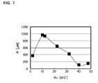
- FIG. 7 is a graph showing the relationship between variable resistance and generated power
- FIG. 8A is an oscilloscope waveform chart at maximum power output
- FIG. 8B is a simulation waveform of output voltage Vm versus gap distance G
- FIG. 9 is a comparison diagram of generating capacity according to the state of electrical connection at the back surface of a dielectric body
- FIG. 10 is a schematic diagram showing a second configuration example of a power generation device
- FIG. 11 is a schematic diagram showing a third configuration example of a power generation device
- FIG. 12 is a schematic diagram showing a first packaging example of a power generation device
- FIG. 13 is a schematic diagram showing a second packaging example of a power generation device
- FIG. 14 is a schematic diagram showing a third packaging example of a power generation device
- FIG. 15 is a schematic diagram showing a fourth packaging example of a power generation device
- FIG. 16 is a schematic diagram showing a fifth packaging example of a power generation device
- FIG. 17 is a schematic diagram showing a sixth packaging example of a power generation device
- FIG. 18 is a schematic diagram showing a seventh packaging example of a power generation device
- FIG. 19 is a schematic diagram showing an eighth packaging example of a power generation device.
- FIG. 20 is a schematic diagram showing a first guide example of a dielectric body
- FIG. 21 is a schematic diagram showing a second guide example of a dielectric body
- FIG. 22 is a schematic diagram showing a first implementation example of a ground ring
- FIG. 23 is a schematic diagram showing a second implementation example of a ground ring
- FIG. 24 is a schematic diagram showing an example of a combination of dielectric body shape and lower electrode shape
- FIG. 25 is a schematic diagram showing a first example of lower electrode shape
- FIG. 26 is a schematic diagram showing a second example of lower electrode shape
- FIG. 27 is a schematic diagram showing a third example of lower electrode shape
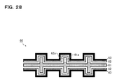
- FIG. 28 is a schematic diagram showing a first structure for realizing triaxial capability
- FIG. 29 is a schematic diagram showing a second structure for realizing triaxial capability
- FIG. 30 is a schematic diagram showing a third structure for realizing triaxial capability
- FIG. 31 is a schematic diagram showing a fourth structure for realizing triaxial capability
- FIG. 32 is a graph showing the relationship between generating capacity and relative permittivity of a dielectric body.
- FIG. 33 is a schematic diagram showing a prior art example of a vibratory power generation device.
- FIG. 1 is a schematic diagram showing a first configuration example of a power generation device (a sectional view seen in a lateral direction).
- the power generation device 10 of the first configuration example has a dielectric body 11 , an electret 12 , a lower electrode 13 , a resistor 14 , an upper electrode 15 , a substrate 16 , and a gap layer 17 .
- the power generation device 10 is depicted in a first state (a state in which the dielectric body 11 and the electret 12 are spaced apart), while at the bottom in FIG. 1 , the power generation device 10 is depicted in a second state (a state in which the dielectric body 11 and the electret 12 are close together).
- the upper edge side of the page is defined as the vertically upward direction, and the description is premised on a configuration in which the dielectric body 11 vibrates in the up-and-down direction (vertical direction); however, the direction of vibration of the dielectric body 11 is not limited thereto; it also being possible, for example, to configure the dielectric body to vibrate in the left-and-right direction (horizontal direction) through 90-degree rotation of the page.
- the dielectric body 11 is a moveable body, the relative position of which varies with respect to the electret 12 due to vibration imparted to the power generation device 10 .
- the bottom face of the dielectric body 11 faces the top face of the electret 12 with the gap layer 17 therebetween.
- Lead zirconate titanate (PZT), barium titanate (BTO), or the like can be employed as the dielectric body 11 . This will be discussed below.
- the dielectric body 11 may be formed to a plate shape or to a film shape.
- the substrate itself may be formed by a dielectric body; a dielectric body film may formed over the substrate by a thin-film printing technique; or a dielectric body of plate shape formed by a separate process may be adhered onto the substrate.
- the electret 12 is a member that retains a quasi-permanent electric charge.
- the electret 12 there may be employed an organic electret that retains an electric charge in a polymer compound, such as CYTOPTM; or an inorganic electret that retains an electric charge in a substrate of silicon oxide (SiO 2 ), silicon nitride (SiN), or the like.
- the electret 12 is formed so as to cover the entire surface of the lower electrode 13 .
- the lower electrode 13 corresponds to a first electrode which is connected to the bottom face side of the electret 12 (the side not facing toward the dielectric body 11 ).
- the lower electrode 13 is connected to a grounding terminal via the resistor 14 .
- An aluminum electrode or the like can be employed as the lower electrode 13 .
- the resistor 14 is a load for drawing, in the form of a voltage, electrical current flowing between the lower electrode 13 and the grounding terminal due to vibration of the power generation device 10 .
- the upper electrode 15 corresponds to a second electrode which is connected to the top face of the dielectric body 11 (the side not facing toward the electret 12 ).
- the upper electrode 15 is directly connected to the grounding terminal.
- An aluminum electrode or the like can be employed as the upper electrode 15 .
- the substrate 16 is a plate-shaped member for supporting the electret 12 and the lower electrode 13 .
- a quartz substrate, a silicon wafer having an oxide film, or the like can be employed as the substrate 16 .
- the gap layer 17 is a gap present between the dielectric body 11 and the electret 12 .
- the thickness of the gap layer 17 (the gap distance separating the dielectric body 11 and the electret 12 ) varies due to displacement of the dielectric body 11 in association with vibration.
- the gap layer 17 may be placed in a low vacuum state (a state that is neither a high vacuum state nor an ultrahigh vacuum state), or filled with air, with an inert gas (N 2 or the like), with a gas having discharge-preventive effect (for example, a gas containing SF 6 as the principal component), or the like.
- a degassing step may be employed, or a phenomenon whereby gas is removed from the gap layer 17 during some high-temperature process, creating a low vacuum state naturally, may be utilized.
- the reason it is undesirable to place the gap layer 17 in a high vacuum state or an ultrahigh vacuum state is so as to avoid discharge of the electret 12 .
- a “low vacuum state” refers to a state of atmospheric pressure to 10 ⁇ 1 Pa
- a “high vacuum state” refers to a state of 10 ⁇ 1 -10 ⁇ 5 Pa
- an “ultrahigh vacuum state” refers to a state of 10 ⁇ 5 Pa or below.
- the power generation device 10 of the first configuration example has at least one dielectric body 11 /electret 12 pair, and is configured to generate power by varying the gap distance between the dielectric body 11 and the electret 12 .
- the basic principle of power generation is described below.
- intrametallic positive charges With the power generation device 10 in the first state (a state in which the dielectric body 11 and the electret 12 are spaced apart) as shown at the top in FIG. 1 , attracted by negative fixed charges (in FIG. 1 , portrayed as symbols of white squares with minus signs) held by the electret 12 , intrametallic positive charges (in FIG. 1 , portrayed as symbols of white circles with plus signs) are induced on the surface of the lower electrode 13 (the interface with the electret 12 ). These intrametallic positive charges assume the character of positive charges that arise as a result of free electrons being expelled from sites within the lower electrode 13 (metal), creating potential difference from surrounding free electrons.
- FIG. 1 shows a state subsequent to movement of a portion of the positive charges from the lower electrode 13 .
- the remaining charges that have not flowed out from the lower electrode 13 are denoted by Q 1 .
- the second state of the power generation device 10 is a state of lower electrostatic potential energy than the first state (a stable state in which distances between positive charges and negative charges are closer together than in the first state). Consequently, when the power generation device 10 is transitioned between the first state and the second state by imparting kinetic energy (vibration) from the outside, it is possible for kinetic energy to be converted to electrical energy.
- the power generation device 10 of the first configuration example is configured to be furnished with the upper electrode 15 on the top face of the dielectric body 11 , with this upper electrode 15 connected to the grounding terminal. Because of this configuration, in the second state of the power generation device 10 , no potential difference arises in the interior of the upper electrode 15 , and therefore it is possible to drag down the potential energy of the second state, and increase the generation efficiency.
- FIG. 2 is an equivalent circuit diagram of the power generation device 10 .
- Sign C 1 shows electrostatic capacitance (fixed value) of the electret 12
- sign C 2 shows electrostatic capacitance (fixed value) of the dielectric body 11
- sign C 3 shows electrostatic capacitance (variable value) of the gap layer
- Sign R shows the resistance value (fixed value) of the resistor 14 .
- the electret 12 which fulfills the role of the power supply, should be called a “constant charge supply” that retains a constant charge Q.
- Equation (1) Q 1 +Q 2 (1)
- Equation (3) the electrostatic capacitance C 1 and the charge Q of the electret 12 are fixed values, whereas the serial composition of capacitance C 4 of the dielectric body 11 and the gap layer 17 is a variable value that varies depending on the thickness of the gap layer 17 (and, hence, on the electrostatic capacitance C 3 of the gap layer 17 ). Consequently, as the serial composition of capacitance C 4 varies in response to displacement of the dielectric body 11 in association with vibration, the ratio of charge Q 2 and charge Q 1 will vary. In the power generation device 10 , the redistribution of charge associated with this change in capacitance is drawn out as electrical current.
- Generating capacity is formulated as follows.
- the electrical current i flowing through a circuit at given time t is given by the time derivative of the charge Q 1 .
- the time derivative of a given function f is denoted by f′
- the electrical current i is represented by the following Equation (4), based on the aforementioned Equation (3):
- ⁇ ′ ⁇ Q ⁇ C ⁇ ⁇ 1 ⁇ ⁇ ( C ⁇ ⁇ 1 + C ⁇ ⁇ 4 ) - 1
- ⁇ ′ ⁇ Q ⁇ C ⁇ ⁇ 1 ⁇ ⁇ - ( C ⁇ ⁇ 1 + C ⁇ ⁇ 4 ) - 2 ⁇ ⁇ C ⁇ ⁇ 4 ′ ( 4 )
- the serial composition of capacitance C 4 of the gap layer 17 is represented by the following Equation (5), employing the electrostatic capacitance C 2 of the dielectric body 11 and the electrostatic capacitance C 3 of the gap layer 17 :
- C 4 ( C 2 ⁇ 1 +C 3 ⁇ 1 ) ⁇ 1 (5)
- Equation (6) the time derivative C 4 ′ of the serial composition of capacitance C 4 is represented by the following Equation (6):
- the electrostatic capacitance C 3 of the gap layer 17 simultaneously varies as well.
- the gap distance of the dielectric body 11 and the electret 12 in the initial state is denoted as X 0
- the dielectric body 11 is experiencing simple harmonic motion at an amplitude A and an angular velocity ⁇
- the capacitance C 3 of the gap layer 17 and the time derivative C 3 ′ thereof are represented by Equation (7) and Equation (8).
- the sign ⁇ 0 in the equations is the dielectric constant of a vacuum (8.85 ⁇ 10 ⁇ 12 F/m).
- the power P drawn from the resistor 14 is represented by Equation (10), employing the average value I of the electrical current i and the resistance value R of the resistor 14 .
- FIG. 8B Simulation values of output voltage waveforms based on the aforementioned Equation (9) are shown in FIG. 8B .
- An output waveform based on this formulation is not a sine wave, but rather a waveform theoretically distorted from a sine wave (discussed in detail below).
- the gap layer 17 present between the dielectric body 11 and the electret 12 plays a useful role.
- the power generation device 10 of the first configuration example differs from the prior art configuration in which the electret and the opposite electrode face one another (see FIG. 33 ), in that the dielectric body 11 and the electret 12 face one another, and therefore even if the dielectric body 11 and the electret 12 are close (or touching), discharge of the electret 12 basically does not arise.
- the dielectric body 11 and the electret 12 when generating power in response to changes in the gap distance separating the dielectric body 11 and the electret 12 , the dielectric body 11 and the electret 12 can be brought closer together until the gap distance reaches its minimum of zero, whereby it is possible to obtain extremely large generating capacity (on a milliwatt scale).
- FIG. 3 is a simplified diagram of a measurement system employed in a power generation test.
- the measurement system X employed in this power generation test includes a dielectric body X 1 , an aluminum panel X 2 , an electromagnetic type vibration exciter X 3 , a test sample X 4 , an aluminum panel X 5 , a three-axis stage X 6 , a base X 7 , a coaxial cable X 8 , a coaxial cable X 9 , a shield case X 10 , a coaxial cable X 11 , a low-pass filter X 12 , a coaxial cable X 13 , and an oscilloscope X 14 .
- the dielectric body X 1 (which corresponds to the dielectric body 11 of FIG. 1 ) is arranged with the top face facing towards the bottom surface of the test sample X 4 , and the bottom surface is connected to the aluminum panel X 2 .
- Lead zirconate titanate (PZT) is employed as the dielectric body X 1 (the dielectric constant of the PZT used in the test is 2,600).
- the aluminum panel X 2 (which corresponds to the upper electrode 15 of FIG. 1 ) is connected at the top surface thereof to the dielectric body X 1 .
- the aluminum panel X 2 is directly connected to the grounding terminal of the measurement system X.
- the electromagnetic type vibration exciter X 3 imparts vibration (of 40 Hz frequency) in the up-and-down direction to the dielectric body X 1 which is connected to the top surface of the aluminum panel X 2 .
- the test sample X 4 (which corresponds to the electret 12 , the lower electrode 13 , and the substrate 16 of FIG. 1 ) is connected at a quartz substrate at the upper surface side thereof (thickness: 1.0 mm) to the aluminum panel X 5 , while an electret at the lower surface side thereof (thickness: 5.6 ⁇ m) faces towards the dielectric body X 1 .
- CYTOPTM is employed as the electret. No patterning has been carried out on the electret. Meanwhile, patterning to pectinate array shape (width: 30 ⁇ m, pitch: 60 ⁇ m) has been carried out on the lower electrode, which is covered by the electret.
- the lower electrode is connected to a first terminal of the coaxial cable X 8 .
- the aluminum panel X 5 provides support to the test sample X 4 .
- test sample X 4 supported on the aluminum panel X 5 is moved in three axial directions by the three-axis stage X 6 .
- the base X 7 provides support to the three-axis stage X 6 .
- the coaxial cable X 8 is connected at a first terminal thereof to the lower electrode of the test sample X 4 , and at a second terminal thereof to a first terminal of the coaxial cable X 9 .
- the coaxial cable X 9 is connected at a first terminal thereof to a second terminal of the coaxial cable X 8 , and at a second terminal thereof to a first connector X 10 a of the shield case X 10 .
- the shield case X 10 houses load resistances Rv, R (the resistor 14 of FIG. 1 corresponds to the serial composition of resistance of Rv and R).
- the main body of the shield case X 10 is connected to the grounding terminal of the measurement system X.
- the first connector X 10 a of the shield case X 10 is connected to the grounding terminal of the measurement system X via the load resistances Rv, R.
- the test sample X 4 and the load resistances Rv, R are connected by a coaxial wire, not by a lead wire.
- the connection node of the load resistances Rv, R connects to a second connector X 10 b of the shield case X 10 as the measurement node for output voltage Vm.
- the ground line of the second connector X 10 b is connected to the grounding terminal of the measurement system X.
- the resistance Rv that is connected between the first connector X 10 a and the second connector X 10 b (the resistance for which voltage at either terminal is not measured) is a variable resistance (a potentiometer)
- the resistance R that is connected between the second connector X 10 b and the grounding terminal (the resistance for which voltage at either terminal is measured as the output voltage Vm) is a fixed resistance (100 k ⁇ ).
- the coaxial cable X 11 connects the second connector X 10 b of the shield case X 10 and the input terminal of the low-pass filter X 12 .
- the low-pass filter X 12 eliminates noise that overlaps the output voltage Vm.
- the cutoff frequency fc of the low-pass filter X 12 is set to 200 Hz.
- the coaxial cable X 13 connects the output terminal of the low-pass filter X 12 and the input terminal of the oscilloscope X 14 .
- the oscilloscope X 14 displays the waveform of the output voltage Vm (temporal variation of the electrical signal) in the form of a graph.
- the vertical axis is output voltage
- the horizontal axis is time.
- the ground terminal of the oscilloscope X 14 is connected to the grounding terminal of the measurement system X.
- Step S 1 a corona discharge device Y shown in FIG. 4 is employed under predetermined conditions (corona discharge voltage: 10 kV, 0.1 mA; grid voltage: 1.5 kV) to introduce a charge into the electret of the test sample X 4 .
- signs X 41 , X 42 , and X 43 respectively show the constituent elements (the electret, the lower electrode, and the substrate) that form the test sample X.
- Signs Y 1 to Y 4 respectively show the constituent elements (a grid, a discharge electrode needle, a grid power supply, a DC high voltage power supply) forming the corona discharge device Y.
- Step S 2 the surface potential of the test sample X 4 is measured.
- Step S 3 the test sample X 4 is connected to the measurement system X.
- Step S 4 the dielectric body X 1 is vibrated by the electromagnetic type vibration exciter X 3 .
- Step S 5 the waveform of the output voltage Vm arising in response to the dielectric body X 1 and the test sample X 4 moving closer together/apart is observed with the oscilloscope.
- Step S 6 Step S 4 to Step S 6 are repeated while varying the resistance value of the variable resistance Rv.
- Step S 7 the output power P of the power generation device 10 is calculated based on the output voltage Vm thusly obtained.
- Vms T ⁇ 1 ⁇ 0 T Vmdt (11)
- VL Vms ⁇ ( R+Rv )/ R (12)
- the generated power P can be calculated from the voltage VL.
- P VL 2 /( R+Rv ) (13)
- Step S 1 the average potential at the test sample X 4 surface was approximately ⁇ 525 V.
- FIG. 5 is a table showing the relationship among variable resistance Rv (Me), maximum amplitude Vpp of the output voltage Vm (V), and generated power Pm ( ⁇ W).
- FIG. 6 is a graph showing the relationship between variable resistance Rv (M ⁇ ) and maximum amplitude Vpp of the output voltage Vm (V).
- FIG. 8A is an oscilloscope waveform chart at maximum power output.
- the driving waveform of a vibration simulator is shown at top in FIG. 8A .
- the dielectric body X 4 provided to the electromagnetic type vibration exciter X 3 experiences simple harmonic motion.
- the output waveform of the output voltage Vm is depicted at bottom in FIG. 8A .
- the output waveform of the output voltage Vm is a shape that differs from a sine wave. However, this waveform is a theoretically correct waveform, not a sine wave distorted by disturbance elements such as noise. This will be described in the next section.
- FIG. 8B is a simulation waveform of the output voltage Vm versus the gap distance G.
- the gap distance of the test sample X 1 and the dielectric body X 4 is depicted at the top in FIG. 8B
- the output voltage Vm of the measurement system X theoretically calculated employing the previously cited Equation (3) to Equation (9) is depicted at the bottom in FIG. 8B .
- numerical values identical to the parameters belonging to the test sample X 1 , the dielectric body X 4 , and the resistances R and Rv employed in the measurement system X used in the actual power generation test were input.
- FIG. 9 is a comparison diagram of generating capacity according to the state of electrical connection at the back surface of the dielectric body X 1 .
- FIG. 9 it was verified that, between the case in which the aluminum plate X 2 is connected to the grounding terminal (the black bar graph) in the measurement system X versus the case in which it is not connected (the hatched bar graph), differences arise both in the maximum amplitude Vpp of the output voltage Vm and in the generated power Pm. This phenomenon will be discussed in detail while citing the following second configuration example and third configuration example.
- FIG. 10 is a schematic diagram showing a second configuration example of a power generation device.
- the power generation device 10 of the second configuration example is substantially analogous in configuration to that of the first configuration example, but has the feature that the upper electrode 15 that was furnished on the top surface side of the dielectric body 11 has been removed.
- the power generation device 10 of the second configuration example can be considered to have a configuration in which the dielectric body 11 is unconnected to any electrode.
- the power generation device 10 of the second configuration example can be considered to have a configuration in which the entire movable section, including the dielectric body 11 , is in an electrically floating state (a state of being unconnected to any potential point).
- the entire movable section, including the dielectric body 11 may be retained by, for example, an insulator (an insulating spring or the like).
- the power generation device 10 of the second configuration example differs from the preceding first configuration example in that, in the second state in which the dielectric body 11 and the electret 12 are brought close together (at bottom in FIG. 10 ), it assumes a state of high electrostatic potential energy (an unstable state), and therefore the generating capacity drops in comparison with the first configuration example.
- the power generation device 10 of the second configuration example does not require wiring to be connected to the vibrating dielectric body 11 , and therefore it is more advantageous than the first configuration example in terms of the ease of device fabrication and the stability of the power generation operation.
- FIG. 11 is a schematic diagram showing a third configuration example of a power generation device.
- the power generation device 10 of the third configuration example is substantially analogous in configuration to that of the first configuration example, but has the feature that a metal body 18 in an electrically floating state is formed on the top surface side of the dielectric body 11 .
- the metal body 18 is a member made of metal, and differs from the upper electrode 15 which was intended to be connected to some potential point (grounding terminal), in that it is in an electrically floating state. Consequently, the power generation device 10 of the third configuration example has in common with the preceding second configuration example a configuration whereby the entire moveable section that includes the dielectric body 11 is in an electrically floating state.
- the metal body 18 may be plate-shaped or film shaped.
- the power generation device 10 of the third configuration example differs from the previously discussed first configuration example in that, because the metal body 18 is not connected to a grounding terminal, positive charges cannot be attracted to the metal body 18 from the grounding terminal. However, because multiple free electrons (in FIG. 11 , depicted as symbols having white circles with minus signs) are present in the metal body 18 , these free electrons move away from the interface of the metal body 18 and the dielectric body 11 , whereby an effect analogous to that when positive charges are attracted the metal body 18 from the grounding terminal is obtained.
- the power generation device 10 of the third configuration example Due to the aforementioned effect, it is possible with the power generation device 10 of the third configuration example to obtain higher generating capacity than with the second configuration example from which the upper electrode 15 has been completely eliminated. In the power generation device 10 of the third configuration example, however, the aforementioned effect is hindered by bias (potential difference) of the charges arising in the interior of the metal body 18 . Consequently, in the power generation device 10 of the third configuration example, the generating capacity declines in comparison to the first configuration example in which the upper electrode 15 is connected to a grounding terminal.
- the first configuration example is superior to the third configuration example, which is in turn superior to the second configuration.
- the second configuration example is equal to the third configuration example, and these are superior to the first configuration example. Consequently, with regard to the configuration of the power generation device 10 , no one configuration can be considered to be always the best, and it is preferable to adopt any of the first to third configurations according to a particular application or required characteristics.
- FIG. 12 is a schematic diagram showing a first packaging example of a power generation device (a cross sectional view taken from a lateral direction).
- the power generation device 20 of the first packaging example has a substrate 21 , a lower electrode 22 , an electret 23 , a dielectric body 24 (in which a dielectric body, electrodes, and a weight are unified), a package 25 , an adhesive 26 , and a wire 27 .
- the lower electrode 22 is formed on the top surface of the substrate 21 .
- the electret 23 is formed so as to cover the lower electrode 22 .
- One terminal of the lower electrode 22 is exposed from the electret 23 , extends out to a terminal section of the substrate 21 , and is connected to the wire 27 in the terminal section.
- the wire 27 is connected to a grounding terminal via a resistor, not shown.
- the package 25 is a cover member (a hollow cylinder, a hollow post, a half sphere, or the like) furnished at one surface with an opening, and the opening is bonded by the adhesive 26 to the substrate 21 , with the electret 23 and the dielectric body 24 housed in the interior thereof.
- the package 25 may be made of a plastic such as a resin or acrylic.
- the dielectric body 24 is unsupported in any way, but rather is housed displaceably (moveably up and down) along the inner wall of the package 25 .
- the dielectric body 24 is close to the electret 23 due to electrostatic attraction (this corresponds to the second state at bottom in FIG. 1 ). Consequently, by imparting kinetic energy (vibration) from the outside in order to move the dielectric body 24 away from the electret 23 , it is possible to convert kinetic energy to electrical energy.
- FIG. 13 is a schematic diagram showing a second packaging example of a power generation device.
- the configuration of the second packaging example is substantially analogous to that of the first packaging example, but has the feature of having an elastic member 31 that pendently supports the dielectric body 24 in the interior of the package 25 .
- a coil spring or an accordion spring (meander configuration) may be employed as the elastic member 31 .
- FIG. 14 is a schematic diagram showing a third packaging example of a power generation device.
- the configuration of the third packaging example is substantially analogous to that of the first packaging example, but has the feature of having elastic members 32 that support both terminals of the dielectric body 24 in the interior of the package 25 .
- Coil springs or accordion springs may be employed as the elastic members 32 .
- FIG. 15 is a schematic diagram showing a fourth packaging example of a power generation device.
- the configuration of the fourth packaging example is substantially analogous to that of the first packaging example, but has the feature of having an elastic member 33 whereby the dielectric body 24 is repulsed from the roof surface of the package 25 .
- a plate spring may be used as the elastic member 33 .
- FIG. 16 is a schematic diagram showing a fifth packaging example of a power generation device (a cross sectional view in a direction from the top).
- the configuration of the fifth packaging example is substantially analogous to that of the first packaging example, but has the feature of having elastic members 34 that support up-and-down motion of the dielectric body 24 while minimizing horizontal movement thereof in the interior of the package 25 .
- the dielectric body 24 and the package 25 are formed to a cross section of rectangular shape in plan view.
- the elastic members 34 it is possible to employ a combination of four plate springs (in a spring arrangement shaped as an equilateral cross with four arms bent at right angles) providing cantilever support of the four side surfaces of the dielectric body 24 from respectively orthogonal support surfaces (inside surfaces of the package 25 ). By adopting this kind of configuration, it is possible to prevent contact of the dielectric body 24 and the top surfaces of the package 25 , without hampering up-and-down motion of the dielectric body 24 .
- FIG. 17 is a schematic diagram showing a sixth packaging example of a power generation device.
- the configuration of the sixth packaging example is substantially analogous to that of the first packaging example, but has the feature of having magnets 35 a and 35 b (a magnetic force spring) for repulsing the dielectric body 24 and the package 25 from one another.
- magnets 35 a and 35 b a magnetic force spring
- FIG. 18 is a schematic diagram showing a seventh packaging example of a power generation device.
- the configuration of the seventh packaging example is substantially analogous to that of the first packaging example, but has the feature of having magnets 36 a and 36 b (a magnetic force spring) for repulsing the dielectric body 24 and the electret 23 from one another.
- magnets 36 a and 36 b a magnetic force spring
- FIG. 19 is a schematic diagram showing an eighth packaging example of a power generation device.
- the configuration of the eighth packaging example is substantially analogous to that of the first packaging example, but has the feature of having a stopper 37 protruding from the surface of the electret 23 .
- the stopper 37 may be furnished on the surface of the dielectric body 24 as well.
- any combination of the configurations described individually in the aforementioned first to eighth packaging examples is possible as well.
- the spring constant such that the inherent resonance frequency of the spring matches the frequency of the vibration imparted to the power generation device 20 .
- FIG. 20 is a schematic diagram showing a first guide example of a dielectric body (a top view, and a cross sectional view from a lateral direction).
- the dielectric body 24 and the package 25 are formed such that their respective outside edges and inside edges are circular, when the power generation device 20 is seen in plan view.
- the dielectric body 24 is housed in an arrangement in which ball members 38 (steel spheres) are wedged between it and the inner wall of the package 25 .
- the ball members 38 are respectively furnished at four equidistant positions along the outer rim of the dielectric body 24 (the inner rim of the package 25 ) when the power generation device 20 is seen in plan view.
- Rail slots 24 a are respectively formed in the up-and-down direction in the dielectric body 24 , at the positions of abutment with the ball members 38 .
- recessed sphere-receiving sections 25 a are respectively formed on the inner wall of the package 25 , at the positions of abutment with the ball members 38 .
- FIG. 21 is a schematic diagram showing a second guide example of a dielectric body (a top view, and a cross sectional view from a lateral direction).
- the power generation device 20 of the second guide example is analogous to the first guide example in that the dielectric body 24 and the package 25 are formed such that their respective outside edges and inside edges are circular, when the power generation device 20 is seen in plan view.
- the dielectric body 24 is housed by an arrangement in which rail members 39 abut the inner wall of the package 25 .
- the rail members 39 are respectively furnished at four equidistant positions along the outer rim of the dielectric body 24 (the inner rim of the package 25 ) when the power generation device 20 is seen in plan view.
- Rail slots 25 b are respectively formed in the up-and-down direction on the wall of the package 25 , at the positions of abutment with the rail members 39 .
- the rail members 39 may be integrally formed by machining of the dielectric body 24 , or formed separately from a material different from the dielectric body 24 and having good slide properties (a fluoroplastic or the like).
- FIG. 22 is a schematic diagram showing a first implementation example of a ground ring (a cross sectional view from a lateral direction).
- the arrows in the drawing show lines of electric force.
- the power generation device 40 of the first implementation example has a dielectric body 41 , an electret 42 , a lower electrode 43 , a resistor 44 , and a ground ring 45 .
- the ground ring 45 is a conductive member (for example, aluminum) formed so as to encircle the perimeter of the electret 42 and the lower electrode 43 , at a predetermined distance away therefrom.
- the ground ring 45 is directly connected to a grounding terminal.
- FIG. 23 is a schematic diagram showing a second implementation example of a ground ring (a cross sectional view from a lateral direction).
- the arrows in FIG. 23 show lines of electric force.
- the ground ring 45 it is not essential for the ground ring 45 to be formed so as to encircle the perimeter of the electret 42 and the lower electrode 43 ; the ground ring 45 and the electret 42 may instead be disposed alternately in mutually adjacent fashion.
- FIG. 24 is a schematic diagram showing an example of a combination of dielectric body shape and lower electrode shape.
- the power generation device 50 of the present example has a dielectric body 51 , an electret 52 , a lower electrode 53 , and a substrate 54 .
- the dielectric body 51 may have a configuration in which the bottom surface that faces the electret 52 has been planarized (see the left side in FIG. 24 ), or a configuration in which the bottom surface has been patterned (see the right side in FIG. 24 ).
- the gap distance of the dielectric body 51 and the electret 52 can be made uniform.
- lines of electric force easily concentrate at sites that have been sharpened through patterning, and improved generation efficiency through optimization of patterning can be anticipated.
- the lower electrode 53 may be formed to a planar shape, without patterning being performed ( FIG. 25 ); or patterning may be carried out to form a pectinate shape ( FIG. 26 ) or spiral shape ( FIG. 27 ). However, from the standpoint of generation efficiency, it is preferable to adopt the former configuration.
- the combination of the shape of the dielectric body 51 (patterned or non-patterned) and the shape of the lower electrode (patterned or non-patterned) is arbitrary.
- FIG. 28 is a schematic diagram showing a first structure for realizing triaxial capability.
- the power generation device 60 of the first structure has a dielectric body 61 , electrets 62 , and a lower electrode 63 .
- a plurality of protruding portions 61 a are formed on the dielectric body 61
- a plurality of recessed portions 62 a adapted to mate with the protruding portions 61 a are formed at predetermined intervals on the electrets 62 .
- the power generation device 60 has an analogous structure in the depthwise direction of the page as well.
- the gap distance of the dielectric body 61 and the electrets 62 may be made to vary in cases in which the dielectric body 61 vibrates in the up-and-down direction of the page, in cases in which the dielectric body 61 vibrates in the left-and-right direction of the page, and in cases in which the dielectric body 61 vibrates in the depthwise direction of the page, whereby it becomes possible to generate power efficiently.
- the electrets 62 are respectively disposed to either side of the dielectric body 61 .
- the dielectric bodies 61 are stacked in multiple layers with the electrets 62 disposed to either side of each, further improvement in generation efficiency can be anticipated. It is of course possible to implement such a multilayer structure in the basic structure discussed previously (in FIG. 1 , etc.), that lacks the protruding portions 61 a and the recessed portions 62 a.
- FIG. 29 is a schematic diagram showing a second structure for realizing triaxial capability.
- an electret 72 is formed on the inner wall of a hermetic container, and particles of a dielectric body 71 are sealed inside the hermetic container.
- a lower electrode 73 is formed so as to encircle the outside peripheral side of the electret 72 , and is connected to a grounding terminal via a resistor 74 .
- FIG. 30 is a schematic diagram showing a third structure for realizing triaxial capability.
- an electret 82 is formed on the inner wall of a hermetic spherical body, and a spherical dielectric body 81 is sealed inside the hermetic spherical body.
- a lower electrode 83 is formed so as to encircle the outside peripheral side of the electret 82 , and is connected to a grounding terminal via a resistor 84 .
- FIG. 31 is a schematic diagram showing a fourth structure for realizing triaxial capability.
- a dielectric body 91 is given a spherical shape, and a plurality of electrets 92 are formed so as to encircle the dielectric body 91 .
- a lower electrode 93 is formed on each of the plurality of electrets 92 , and is connected to a grounding terminal via a resistor 84 .
- FIG. 32 is a graph showing the relationship between generating capacity and relative permittivity of a dielectric body.
- the horizontal axis of FIG. 32 shows the relative permittivity Er of a dielectric body, and the vertical axis of FIG. 32 shows the generating capacity P (%) (normalized using the generating capacity in a case in which the relative permittivity ⁇ r is infinite).
- the present graph shows computation results obtained by the previously cited Equations (3) to (9), under hypothetical conditions of an electret relative permittivity of 2, an electret film thickness of 5 ⁇ m, a dielectric body vibration amplitude of 20 ⁇ m, and a gap layer (an air layer) thickness (gap distance) of 1 ⁇ m, when the dielectric body and the electret are closest.
- the generated power outputs in the drawing have been normalized using a generating capacity of 100% in a case in which the relative permittivity ⁇ r of the dielectric body is infinite.
- the circle symbols, square symbols, and diamond symbols in FIG. 32 respectively show computation results when the thickness of the dielectric body was 0.01 mm, 0.1 mm, and 1 mm.
- the computation results vary according to the thickness of the dielectric body.
- maximum generating capacity of 90% is obtained when the relative permittivity ⁇ r is approximately 30.
- relative permittivity ⁇ r is necessary to obtain maximum generating capacity of 90%. Consequently, in order to increase the generating capacity, it is preferable for the dielectric body to be as thin as possible.
- the dielectric body may suitably employ a material having a thickness of 0.01 to 1.0 mm (preferably 0.01 to 0.1 mm), and from which maximum generating capacity of 80% or more can be obtained.
- dielectric bodies of a thickness of one micron or less to several microns can be fabricated by a sputtering process or electron beam deposition process.
- Dielectric bodies of a thickness of one micron or less to several tens of microns can be fabricated by a hydrothermal synthesis process including a sol-gel process, accompanied by spin coating and firing.
- Dielectric bodies of a thickness of several tens of microns or more can be fabricated by firing of a powder, pressure molding or another molding process, and thickness adjustment by slicing, cutting, polishing, or the like.
- the most desirable material is barium titanate (BaTiO 3 , BTO).
- the relative permittivity at service temperatures (expected to be 0 to 100° C.) is approximately 1,000, which meets the aforementioned condition.
- the material is relatively cheap, and has minimal environmental impact by virtue of being lead-free, and is therefore advantageous for commercial purposes as well.
- the relative permittivity drops.
- the relative permittivity drops in cases in which the operating frequency is 100 kHz or above.
- the expected operating frequency is from 1 to several hundred Hz, the aforementioned characteristics are not a drawback for the present device.
- the only problem is that, by virtue of being a ferroelectric body, there is hysteresis in the dielectric characteristics.
- the next most desirable material is lead zirconate titanate (PZT). Because of the extremely high relative permittivity (2,000 to 3,000), the material is effective in cases in which it is desired to make the generating capacity as great as possible. However, drawbacks are relatively high cost, and high environmental impact by virtue of containing lead. Moreover, like barium titanate, it is a ferroelectric body, and it is necessary to be aware of hysteresis in the characteristics.
- alkaline earth metals such as potassium (K), calcium (Ca), strontium (Sr) or the like, or rare earth metals such as yttrium (Yt), neodymium (Nd), or the like, to barium titanate.
- K potassium
- Ca calcium
- Sr rare earth metals
- Yt yttrium
- Nd neodymium
- a first effect is to depress the Curie temperature.
- a ferroelectric body has a unique temperature, known as the Curie temperature, in proximity to which temperature the maximum permittivity is observed. Consequently, by setting the Curie temperature of a dielectric body to closely approximate the service temperature of the power generation device, the permittivity at operating temperature can be increased to a level greater than that of pure barium titanate.
- permittivity varies considerably with temperature variations, and destabilized generation efficiency is a drawback.
- a second effect is that as the added amount is increased, the nature of the material varies from a ferroelectric body to a paraelectric body.
- a paraelectric body exhibits minimal variation of permittivity due to temperature variations, and lacks hysteresis, and therefore stable power generation can be anticipated. Due to permittivity that is high among paraelectric bodies, a modicum of generating capacity can be assured.
- Strontium titanate is the result of substituting strontium for barium in barium titanate.
- the material is a ferroelectric body, with permittivity of approximately 300, and has the advantage of meeting the aforementioned condition.
- the permittivity is low in comparison with barium titanate.
- strontium is a rare metal, and is costly.
- lanthanum iron oxide LaFeO 3
- KNbO 3 potassium niobate
- LaTiO 3 lanthanum titanate
- MgSiO 3 magnesium silicate
- Ba(Ti, Zr)O 3 barium titanate zirconate
- a characteristic of lanthanum iron oxide (LaFeO 3 ) is that the relative permittivity of a monocrystal layer is 1,000 or above, with the relative permittivity reaching several tens of thousands or more at high temperatures.
- the addition of a trace amount of lanthanum iron oxide (LaFeO 3 ) to potassium niobate (KNbO 3 ) has the effect of pulling up the permittivity.
- addition of 0.2% lanthanum iron oxide (LaFeO 3 ) boosts the relative permittivity of potassium niobate (KNbO 3 ) at room temperature from 500 to 1,250.
- the crystalline structure of potassium niobate is a perovskite structure. At ⁇ 10° C. or below it is rhombohedral, but at normal temperature it becomes orthorhombic, at 225 to 435° C. it becomes tetragonal, and at 435° C. (the Curie temperature) and above it becomes cubic.
- the material is a ferroelectric body and shows high piezoelectricity
- the material is a ferroelectric body having a bismuth layer structure, as well as being a lead-free piezoelectric ceramic
- the material is easily polarized (polarization at 5 to 6 kV/mm or less at 150° C.
- the material has relative permittivity (800 to 1,000) comparable to that of lead zirconate titanate (PZT); and (5) the material has a relatively flat relative permittivity curve from room temperature up to about 200° C.
- PZT lead zirconate titanate
- polylactic acid and polyureic acid there may be cited polylactic acid and polyureic acid.
- Polymer-based ferroelectric bodies are pliable and have relatively high permittivity, and therefore applications such as protective films for contact surfaces and the like may be anticipated.
- the relative permittivity of polylactic acid is approximately 22.
- Polyureic acid is an organic piezoelectric material with relative permittivity of 3.6 to 11.8.
- relaxor ferroelectric bodies may be cited.
- characteristics common to relaxor ferroelectric bodies there may be cited: (1) large piezoelectric effects; (2) extremely large permittivity and low temperature variation thereof; (3) anomalously large relative permittivity reaching into the several tens of thousands; (4) having a broad permittivity peak and frequency distribution; and (5) having spontaneous polarization characteristics that show slow variation up to high temperatures.
- Most relaxor ferroelectric bodies have a compound structure of the complex perovskite type (A(B′,B′′)O 3 ) in which divalent ions are present at the A sites, and two different types of ions having on average tetravalent charge are present at the B sites. These may be broadly classified into a type containing ions of +2 valence and +5 valence in a 1:2 ratio (A(B′ 1/3 B′′ 2/3 )O 3 ), and types containing ions of +3 valence and +5 valence or ions of +2 valence and +6 valence in a 1:1 ratio (A(B′ 1/2 B′′ 1/2 )O 3 ). Most relaxor ferroelectric bodies form mixed crystals with the ferroelectric body PbTiO 3 , and give rise to interesting phenomena.
- A(B′,B′′)O 3 complex perovskite type in which divalent ions are present at the A sites, and two different types of ions having on average tetravalent charge are present at the B
- relaxor ferroelectric bodies there may be cited (1 ⁇ x)Pb(Mg 1/3 Nb 2/3 )O 3 .xPbTiO 3 , (1 ⁇ x)Pb(Zn 1/3 Nb 2/3 )O 3 .xPbTiO 3 , and (1 ⁇ x)Pb(In 1/2 Nb 1/2 )O 3 .xPbTiO 3 .
- PZN/xPT As characteristics of solid solutions (PZN/xPT) of Pb(Zn 1/3 Nb 2/3 )O 3 and PbTiO 3 there may be cited: (1) they are ferroelectric bodies and piezoelectric bodies; and (2) in the case of PZN/9PT, the piezoelectric constant d 33 is approximately 2,500 pC/N.
- the compositional ratio of PZN and PT is in a range termed the morphotropic phase boundary (commonly known as the MPB) that exactly divides trigonal from tetragonal, and various experimental techniques are being employed to search for the cause of the high piezoelectric effect, from the standpoint of the drop in symmetry observed at the MPB.
- MPB morphotropic phase boundary
- the material is a lead-free relaxor ferroelectric body.
- the correct composition is (Ba 1-x La x )(Ti 1-x Cr x )O 3 (where 0 ⁇ x ⁇ 1).
- the aforementioned power generation devices as a power supply for sensors of various kinds or wireless devices (for example, ZigBee 300 MHz band-specific low-power wireless devices), there can be built a ubiquitous environment of wireless sensors and a wireless sensor network. Specifically, because the need for power supply wiring for the various sensors and the wireless devices is obviated, it is possible for individual devices to be disposed in dispersed fashion, and to realize information linkages within the network.
- wireless devices for example, ZigBee 300 MHz band-specific low-power wireless devices
- TPMS tire pressure monitoring systems
- TPMS tire pressure monitoring systems
- the medical and health fields health management and safety confirmation
- monitoring of structures monitoring for wire disconnects or loose bolts
- monitoring plants monitoring for equipment faults
- logistics management monitoring logistics and product quality
- motors and other such electrical machinery vibrate at the power supply frequency (50 Hz or 60 Hz)
- the resonance condition of a spring system incorporated into a power generation device is matched to the aforementioned power supply frequency
- even larger generating capacity can be anticipated, and therefore use of the generated power output as a power supply of a data processing device or the like is conceivable.
- applications in which the aforementioned power generation devices are attached to the body to generate power or applications in which the aforementioned power generation devices are installed in a mobile device such as a mobile telephone, may be envisioned as well.
- power is generated from Z-axis component vibration of a vibrator, thereby obviating the need for fine patterning of the electret and the electrodes; and because the dielectric body and the electret do not discharge even if in contact, there is no need to avoid contact of the dielectric body and the electret as well, whereby it is possible to offer a compact, high-output power generation device, and hence possible to relieve the user of any concern about battery life.
- the power generation device is a technique suitably applicable as a power supply employed by various types of sensors and wireless devices (wireless sensor networks, health monitoring, and the like).
Abstract
Description
Q=Q1+Q2 (1)
V=Q1/C1=Q2/C4 (2)
Q1=Q1×C1/(C1+C4) (3)
C4=(C2−1 +C3−1)−1 (5)
C3=∈0×∈r×S×{X0+A×sin(ω×t)}−1 (7)
C3′=−∈0×∈r×S×A×ω×cos(ω×t)×{X0+A×sin(ω×t)}−2 (8)
V2=i×R (9)
P=I 2 ×R=T −1×∫0 Ti 2 dt×R (10)
Vms=T −1×∫0 T Vmdt (11)
VL=Vms×(R+Rv)/R (12)
P=VL 2/(R+Rv) (13)
- 10 Power generation device
- 11 Dielectric body
- 12 Electret
- 13 Lower electrode
- 14 Resistor
- 15 Upper electrode
- 16 Substrate
- 17 Gap layer
- 18 Metal body
- 20 Power generation device
- 21 Substrate
- 22 Lower electrode
- 23 Electret
- 24 Dielectric body (unified dielectric body, electrodes, and weight)
- 24 a Rail slots
- 25 Package
- 25 a Sphere-receiving sections
- 25 b Rail slots
- 26 Adhesive
- 27 Wire
- 31-34 Elastic members
- 35 a, 35 b, 36 a, 36 b Magnets
- 37 Stopper
- 38 Ball member
- 39 Rail member
- 40 Power generation device
- 41 Dielectric body
- 42 Electret
- 43 Lower electrode
- 44 Resistor
- 45 Ground ring
- 50 Power generation device
- 51 Dielectric body
- 52 Electret
- 43 Lower electrode
- 54 Substrate
- 60 Power generation device
- 61 Dielectric body
- 61 a Protruding portions
- 62 Electret
- 62 a Recessed portions
- 63 Lower electrode
- 70, 80, 90 Power generation device
- 71, 81, 91 Dielectric body
- 72, 72, 92 Electret
- 73, 83, 93 Lower electrode
- 74, 84, 94 Resistor
- X1 Dielectric body
- X2 Aluminum plate
- X3 Electromagnetic type vibration exciter
- X4 Test sample
- X41 Electret
- X42 Lower electrode
- X43 Substrate
- X5 Aluminum plate
- X6 Three-axis stage
- X7 Base
- X8 Coaxial cable
- X9 Coaxial cable
- X10 Shield case
- X10 a First connector
- X10 b Second connector
- X11 Coaxial cable
- X12 Low-pass filter
- X13 Coaxial cable
- X14 Oscilloscope
- Rv, R Load resistance
- Y Corona discharge device
- Y1 Grid
- Y2 Discharge electrode needle
- Y3 Grid power supply
- Y4 DC high voltage power supply
Claims (22)
Applications Claiming Priority (2)
| Application Number | Priority Date | Filing Date | Title |
|---|---|---|---|
| JP2011190391A JP5945102B2 (en) | 2011-09-01 | 2011-09-01 | Power generator |
| JP2011-190391 | 2011-09-01 |
Publications (2)
| Publication Number | Publication Date |
|---|---|
| US20130057110A1 US20130057110A1 (en) | 2013-03-07 |
| US9413272B2 true US9413272B2 (en) | 2016-08-09 |
Family
ID=47752589
Family Applications (1)
| Application Number | Title | Priority Date | Filing Date |
|---|---|---|---|
| US13/599,091 Active 2034-03-09 US9413272B2 (en) | 2011-09-01 | 2012-08-30 | Power generation device having a dielectric body and an electret |
Country Status (2)
| Country | Link |
|---|---|
| US (1) | US9413272B2 (en) |
| JP (1) | JP5945102B2 (en) |
Cited By (3)
| Publication number | Priority date | Publication date | Assignee | Title |
|---|---|---|---|---|
| US20160285391A1 (en) * | 2013-03-19 | 2016-09-29 | Tohoku University | Electrostatic induction-type vibration power generation device and method of manufacturing the same |
| CN107482950A (en) * | 2017-09-01 | 2017-12-15 | 天津理工大学 | A kind of miniature friction nano generator of multi-layered electrode superposition |
| US11081285B2 (en) | 2019-05-08 | 2021-08-03 | Deborah Duen Ling Chung | Electrically conductive electret and associated electret-based power source and self-powered structure |
Families Citing this family (26)
| Publication number | Priority date | Publication date | Assignee | Title |
|---|---|---|---|---|
| JP5945102B2 (en) * | 2011-09-01 | 2016-07-05 | 学校法人 関西大学 | Power generator |
| US9843213B2 (en) | 2013-08-06 | 2017-12-12 | Energous Corporation | Social power sharing for mobile devices based on pocket-forming |
| US20140008993A1 (en) | 2012-07-06 | 2014-01-09 | DvineWave Inc. | Methodology for pocket-forming |
| US9831718B2 (en) | 2013-07-25 | 2017-11-28 | Energous Corporation | TV with integrated wireless power transmitter |
| US10008889B2 (en) | 2014-08-21 | 2018-06-26 | Energous Corporation | Method for automatically testing the operational status of a wireless power receiver in a wireless power transmission system |
| US10199849B1 (en) | 2014-08-21 | 2019-02-05 | Energous Corporation | Method for automatically testing the operational status of a wireless power receiver in a wireless power transmission system |
| CN104104261B (en) * | 2013-04-12 | 2016-08-10 | 纳米新能源(唐山)有限责任公司 | Electricity generation system |
| CN104104260B (en) * | 2013-04-12 | 2016-10-12 | 纳米新能源(唐山)有限责任公司 | Electricity generation system |
| CN103780132B (en) * | 2013-07-18 | 2016-02-03 | 北京纳米能源与系统研究所 | A kind of pulse friction generator and triboelectricity method |
| JP6162527B2 (en) * | 2013-08-05 | 2017-07-12 | 達夫 中西 | Power generator |
| JP6377396B2 (en) * | 2014-04-18 | 2018-08-22 | キヤノンメディカルシステムズ株式会社 | Ultrasonic probe |
| JP6581181B2 (en) * | 2014-04-18 | 2019-09-25 | 北京納米能源与系統研究所 | Electrostatic induction sensor, generator, sensing method and power generation method |
| US9973008B1 (en) | 2014-05-07 | 2018-05-15 | Energous Corporation | Wireless power receiver with boost converters directly coupled to a storage element |
| JP6320843B2 (en) * | 2014-05-16 | 2018-05-09 | 学校法人 関西大学 | Power generator |
| CN105515437B (en) * | 2014-10-14 | 2018-06-08 | 北京纳米能源与系统研究所 | Friction generator and the method for application friction generator power generation |
| CN105577024A (en) * | 2014-11-06 | 2016-05-11 | 北京纳米能源与系统研究所 | Vibration type friction generator |
| CN104811090B (en) | 2015-03-30 | 2017-08-29 | 南方科技大学 | A kind of electrostatic energy collecting device and electrostatic energy-collecting method |
| KR102578823B1 (en) | 2016-05-10 | 2023-09-15 | 삼성전자주식회사 | Triboelectric generator |
| US10770990B2 (en) | 2016-05-10 | 2020-09-08 | Samsung Electronics Co., Ltd. | Triboelectric generator |
| JP2018107437A (en) * | 2016-12-27 | 2018-07-05 | キヤノン株式会社 | Vibrator, vibration wave driver, vibration wave motor, and electronic equipment |
| CN108347198B (en) * | 2017-01-25 | 2020-06-16 | 北京纳米能源与系统研究所 | Electret self-generating device and electret self-generating intelligent shoe |
| JP6335347B1 (en) * | 2017-02-09 | 2018-05-30 | 株式会社トライフォース・マネジメント | Power generation element and power generation device |
| CN108429485A (en) * | 2018-03-27 | 2018-08-21 | 中国科学院微电子研究所 | Capsule-type electret generator and energy supply device |
| DE102018221047A1 (en) * | 2018-04-05 | 2019-10-10 | Continental Reifen Deutschland Gmbh | Apparatus for measuring a mechanical force comprising first, second, third, fourth and fifth layers and the uses of the apparatus and tires or engineering rubber articles comprising the apparatus |
| JP2021064690A (en) | 2019-10-11 | 2021-04-22 | 株式会社リコー | Element and method for manufacturing element |
| CN116461257B (en) * | 2023-05-12 | 2024-04-12 | 广东海洋大学 | Tire pressure monitoring device, method and system, wheel and carrier |
Citations (24)
| Publication number | Priority date | Publication date | Assignee | Title |
|---|---|---|---|---|
| JPH0556666A (en) | 1991-08-23 | 1993-03-05 | Ricoh Co Ltd | Guide mechanism for actuator and its manufacture |
| JPH07147786A (en) | 1993-11-25 | 1995-06-06 | Fujitsu Ltd | Electrostatic actuator |
| JP2002165468A (en) | 2000-09-12 | 2002-06-07 | Toshio Sakai | Electrostatic power generation method and apparatus |
| US20040007877A1 (en) * | 2002-06-07 | 2004-01-15 | California Institute Of Technology | Electret generator apparatus and method |
| US20040016120A1 (en) * | 2002-06-07 | 2004-01-29 | California Institute Of Technology | Method and resulting device for fabricating electret materials on bulk substrates |
| JP2004186732A (en) | 2002-11-29 | 2004-07-02 | Hosiden Corp | Electrostatic sensor and portable electronic apparatus |
| JP2006066178A (en) | 2004-08-26 | 2006-03-09 | Nippon Telegr & Teleph Corp <Ntt> | Electrostatic driving switch and manufacturing method of same |
| JP2007312551A (en) | 2006-05-19 | 2007-11-29 | Univ Of Tokyo | Electrostatic induction type converting device |
| US20080048521A1 (en) | 2006-07-28 | 2008-02-28 | Sanyo Electric Co., Ltd. | Electric power generator |
| WO2008026407A1 (en) | 2006-08-31 | 2008-03-06 | Sanyo Electric Co., Ltd. | Electrostatic operation device |
| JP2008086190A (en) | 2006-07-28 | 2008-04-10 | Sanyo Electric Co Ltd | Power generator, electrical equipment mounted with the same, and communications device mounted with the equipment |
| US20090051242A1 (en) * | 2004-11-26 | 2009-02-26 | The University Of Tokyo | Electrostatic induction conversion device |
| US20090079295A1 (en) | 2007-09-26 | 2009-03-26 | Sanyo Electric Co., Ltd. | Electrostatic generator |
| WO2009125773A1 (en) | 2008-04-07 | 2009-10-15 | 国立大学法人埼玉大学 | Electromechanical transducer, electromechanical transducer device, and fabrication method for same |
| JP2010068643A (en) | 2008-09-11 | 2010-03-25 | Nippon Signal Co Ltd:The | Electrostatic induction type power generation device and method for manufacturing the same |
| US20100164322A1 (en) * | 2006-06-16 | 2010-07-01 | Toshiiku Sashida | Electrostatic motor |
| US20110062820A1 (en) * | 2009-09-15 | 2011-03-17 | Rohm Co., Ltd. | Power Generation Apparatus |
| JP2011078198A (en) | 2009-09-30 | 2011-04-14 | Brother Industries Ltd | Electrostatic induction generation apparatus |
| WO2011052106A1 (en) | 2009-10-29 | 2011-05-05 | パナソニック株式会社 | Power generator |
| JP2011101499A (en) | 2009-11-05 | 2011-05-19 | Panasonic Corp | Power generation apparatus |
| WO2011086830A1 (en) | 2010-01-14 | 2011-07-21 | オムロン株式会社 | Electrostatic induction power generator |
| US20110316384A1 (en) * | 2009-12-03 | 2011-12-29 | Hiroshi Nakatsuka | Vibration power generator, vibration power generation device, and electronic device and communication device having viberation power generation device installed |
| US20120169179A1 (en) * | 2008-12-08 | 2012-07-05 | Omron Corporation | Energy conversion device of electrostatic induction type |
| US20130057110A1 (en) * | 2011-09-01 | 2013-03-07 | Kansai University | Power generation device |
-
2011
- 2011-09-01 JP JP2011190391A patent/JP5945102B2/en active Active
-
2012
- 2012-08-30 US US13/599,091 patent/US9413272B2/en active Active
Patent Citations (32)
| Publication number | Priority date | Publication date | Assignee | Title |
|---|---|---|---|---|
| JPH0556666A (en) | 1991-08-23 | 1993-03-05 | Ricoh Co Ltd | Guide mechanism for actuator and its manufacture |
| JPH07147786A (en) | 1993-11-25 | 1995-06-06 | Fujitsu Ltd | Electrostatic actuator |
| US5523639A (en) | 1993-11-25 | 1996-06-04 | Fujitsu Limited | Electrostatic actuator having ferroelectrics in which residual dielectric polarization is formed |
| JP2002165468A (en) | 2000-09-12 | 2002-06-07 | Toshio Sakai | Electrostatic power generation method and apparatus |
| US20040007877A1 (en) * | 2002-06-07 | 2004-01-15 | California Institute Of Technology | Electret generator apparatus and method |
| US20040016120A1 (en) * | 2002-06-07 | 2004-01-29 | California Institute Of Technology | Method and resulting device for fabricating electret materials on bulk substrates |
| JP2005529574A (en) | 2002-06-07 | 2005-09-29 | カリフォルニア インスティテュート オブ テクノロジー | Electret power generation apparatus and method |
| JP2004186732A (en) | 2002-11-29 | 2004-07-02 | Hosiden Corp | Electrostatic sensor and portable electronic apparatus |
| JP2006066178A (en) | 2004-08-26 | 2006-03-09 | Nippon Telegr & Teleph Corp <Ntt> | Electrostatic driving switch and manufacturing method of same |
| US20090051242A1 (en) * | 2004-11-26 | 2009-02-26 | The University Of Tokyo | Electrostatic induction conversion device |
| JP2007312551A (en) | 2006-05-19 | 2007-11-29 | Univ Of Tokyo | Electrostatic induction type converting device |
| US20100164322A1 (en) * | 2006-06-16 | 2010-07-01 | Toshiiku Sashida | Electrostatic motor |
| US20080048521A1 (en) | 2006-07-28 | 2008-02-28 | Sanyo Electric Co., Ltd. | Electric power generator |
| JP2008086190A (en) | 2006-07-28 | 2008-04-10 | Sanyo Electric Co Ltd | Power generator, electrical equipment mounted with the same, and communications device mounted with the equipment |
| WO2008026407A1 (en) | 2006-08-31 | 2008-03-06 | Sanyo Electric Co., Ltd. | Electrostatic operation device |
| US20100019616A1 (en) | 2006-08-31 | 2010-01-28 | Sanyo Electric Co., Ltd. | Electrostatic operation device |
| US20120217842A1 (en) * | 2006-08-31 | 2012-08-30 | Sanyo Electric Co., Ltd. | Electrostatic operation device |
| US20090079295A1 (en) | 2007-09-26 | 2009-03-26 | Sanyo Electric Co., Ltd. | Electrostatic generator |
| JP2009081950A (en) | 2007-09-26 | 2009-04-16 | Sanyo Electric Co Ltd | Electrostatic generating apparatus |
| WO2009125773A1 (en) | 2008-04-07 | 2009-10-15 | 国立大学法人埼玉大学 | Electromechanical transducer, electromechanical transducer device, and fabrication method for same |
| US20110108838A1 (en) | 2008-04-07 | 2011-05-12 | National University Corporation Saitama University | Electro-mechanical transducer, an electro-mechanical converter, and manufacturing methods of the same |
| JP2010068643A (en) | 2008-09-11 | 2010-03-25 | Nippon Signal Co Ltd:The | Electrostatic induction type power generation device and method for manufacturing the same |
| US20120169179A1 (en) * | 2008-12-08 | 2012-07-05 | Omron Corporation | Energy conversion device of electrostatic induction type |
| US20110062820A1 (en) * | 2009-09-15 | 2011-03-17 | Rohm Co., Ltd. | Power Generation Apparatus |
| US8304958B2 (en) * | 2009-09-15 | 2012-11-06 | Rohm Co., Ltd. | Power generation apparatus including an electret and an opposing electrode on the surface of a movable member facing a dielectric |
| JP2011078198A (en) | 2009-09-30 | 2011-04-14 | Brother Industries Ltd | Electrostatic induction generation apparatus |
| WO2011052106A1 (en) | 2009-10-29 | 2011-05-05 | パナソニック株式会社 | Power generator |
| JP2011101499A (en) | 2009-11-05 | 2011-05-19 | Panasonic Corp | Power generation apparatus |
| US20110316384A1 (en) * | 2009-12-03 | 2011-12-29 | Hiroshi Nakatsuka | Vibration power generator, vibration power generation device, and electronic device and communication device having viberation power generation device installed |
| WO2011086830A1 (en) | 2010-01-14 | 2011-07-21 | オムロン株式会社 | Electrostatic induction power generator |
| US20130134830A1 (en) | 2010-01-14 | 2013-05-30 | Omron Corporation | Electrostatic induction power generator |
| US20130057110A1 (en) * | 2011-09-01 | 2013-03-07 | Kansai University | Power generation device |
Non-Patent Citations (2)
| Title |
|---|
| Edamoto et al., "Low-Resonant-Frequency Micro Electret Generator for Energy Harvesting Application," Proc. IEEE Int. Conf. MEMS, pp. 1059-1062, 2009. |
| Naruse et al., "Electrostatic Micro Power Generator From Low Frequency Vibration Such as Human Motion," Proceedings of Power MEMS 2008+ microMEMS 2008, Sendai, Japan, Nov. 9-12, 2008. |
Cited By (5)
| Publication number | Priority date | Publication date | Assignee | Title |
|---|---|---|---|---|
| US20160285391A1 (en) * | 2013-03-19 | 2016-09-29 | Tohoku University | Electrostatic induction-type vibration power generation device and method of manufacturing the same |
| US9929679B2 (en) * | 2013-03-19 | 2018-03-27 | Sendai Smart Machines Co., Ltd. | Electrostatic induction-type vibration power generation device and method of manufacturing the same |
| CN107482950A (en) * | 2017-09-01 | 2017-12-15 | 天津理工大学 | A kind of miniature friction nano generator of multi-layered electrode superposition |
| CN107482950B (en) * | 2017-09-01 | 2019-05-07 | 天津理工大学 | A kind of miniature friction nano generator of multi-layered electrode superposition |
| US11081285B2 (en) | 2019-05-08 | 2021-08-03 | Deborah Duen Ling Chung | Electrically conductive electret and associated electret-based power source and self-powered structure |
Also Published As
| Publication number | Publication date |
|---|---|
| JP2013055724A (en) | 2013-03-21 |
| JP5945102B2 (en) | 2016-07-05 |
| US20130057110A1 (en) | 2013-03-07 |
Similar Documents
| Publication | Publication Date | Title |
|---|---|---|
| US9413272B2 (en) | Power generation device having a dielectric body and an electret | |
| Todaro et al. | Piezoelectric MEMS vibrational energy harvesters: Advances and outlook | |
| Khan et al. | State-of-the-art in vibration-based electrostatic energy harvesting | |
| US8742644B2 (en) | Power generation apparatus | |
| Kim et al. | Piezoelectric energy harvesting | |
| Kakimoto et al. | Fabrication of fibrous BaTiO3-reinforced PVDF composite sheet for transducer application | |
| WO2015174486A1 (en) | Electricity-generating device | |
| Kachroudi et al. | Micro-structured PDMS piezoelectric enhancement through charging conditions | |
| Zhang et al. | Micro energy harvester with dual electrets on sandwich structure optimized by air damping control for wireless sensor network application | |
| Godard et al. | 1-mW vibration energy harvester based on a cantilever with printed polymer multilayers | |
| Cao et al. | Vibration energy harvesting characterization of 1 cm2 Poly (vinylidene fluoride) generators in vacuum | |
| US11041896B2 (en) | Piezoelectric property measuring apparatus for liquid or viscous material | |
| Jagtap et al. | Geometry optimization of a MEMS-based energy harvesting device | |
| Doshida et al. | Double-mode miniature cantilever-type ultrasonic motor using lead-free array-type multilayer piezoelectric ceramics | |
| Lo et al. | Parylene-HT-based electret rotor generator | |
| JP6108137B2 (en) | Power generator | |
| Prakash et al. | Study of effect on resonance frequency of piezoelectric unimorph cantilever for energy harvesting | |
| Zhang et al. | Energy scavenging from vibration with two-layer laminated fluoroethylenepropylene piezoelectret films | |
| Crovetto et al. | MEMS fabricated energy harvesting device with 2D resonant structure | |
| Tao et al. | A three-dimensional electrostatic/electret micro power generator for low acceleration and low frequency vibration energy harvesting | |
| Feng et al. | All-polymer soft-X-ray-charged piezoelectret with embedded PEDOT electrode | |
| Tiwari et al. | Study of different energy scavenging techniques through vibration and its micro power applications | |
| Huang et al. | High Performance Frequency Up-Conversion Energy Harvester Based on PZT Thick Film Technology for IoT Applications | |
| Wu | A sensitivity-enhanced electric field sensor with electrostatic field bias | |
| Asanuma et al. | A spontaneous polarization electret for electrostatic vibration energy harvesting |
Legal Events
| Date | Code | Title | Description |
|---|---|---|---|
| AS | Assignment |
Owner name: ROHM CO., LTD., JAPAN Free format text: ASSIGNMENT OF ASSIGNORS INTEREST;ASSIGNORS:AOYAGI, SEIJI;TAKAHASHI, TOMOKAZU;SUZUKI, MASATO;AND OTHERS;REEL/FRAME:028926/0203 Effective date: 20120803 Owner name: KANSAI UNIVERSITY, JAPAN Free format text: ASSIGNMENT OF ASSIGNORS INTEREST;ASSIGNORS:AOYAGI, SEIJI;TAKAHASHI, TOMOKAZU;SUZUKI, MASATO;AND OTHERS;REEL/FRAME:028926/0203 Effective date: 20120803 |
|
| STCF | Information on status: patent grant |
Free format text: PATENTED CASE |
|
| MAFP | Maintenance fee payment |
Free format text: PAYMENT OF MAINTENANCE FEE, 4TH YEAR, LARGE ENTITY (ORIGINAL EVENT CODE: M1551); ENTITY STATUS OF PATENT OWNER: LARGE ENTITY Year of fee payment: 4 |
|
| FEPP | Fee payment procedure |
Free format text: MAINTENANCE FEE REMINDER MAILED (ORIGINAL EVENT CODE: REM.); ENTITY STATUS OF PATENT OWNER: LARGE ENTITY |